Method of forming organosilicon oxide film and multilayer resist structure

a technology of organosilicon oxide and resist structure, which is applied in the direction of resistive material coating, superimposed coating process, liquid/solution decomposition chemical coating, etc., can solve the problems of low minuteness, poor ashing resistance, and limit the maximum temperature permitted, and achieve excellent ashing resistance, low cost, and high productivity

Active Publication Date: 2007-06-21
ASM JAPAN
View PDF4 Cites 4 Cited by
  • Summary
  • Abstract
  • Description
  • Claims
  • Application Information

AI Technical Summary

Benefits of technology

[0007] Consequently, in an embodiment, an object of the present invention is to form an organosilicon oxide film having excellent ashing resistance even at a low temperature. In another embodiment, an object of the present invention is to form an organosilicon oxide film as an intermediate layer between resist layers without causing plasma damage to a semiconductor device. In still another embodiment, an object of the present invention is to form an organosilicon oxide film at high productivity and at low costs.
[0012] The temperature of the susceptor may be in the range of about 150° C. to about 290° C., preferably about 200° C. to about 280° C., and in another embodiment, about 250° C. or lower. The temperature of the susceptor is substantially or nearly the same as that of the substrate in a typical plasma CVD apparatus. However, if the temperature of the susceptor and that of the substrate are different, the temperature of the substrate needs to be adjusted at the above-indicated temperature. Because the organosilicon oxide film can be formed at a low temperature, plasma damage can effectively be avoided.
[0013] The organosilicon oxide film has excellent ashing resistance and thus it is effective to deposit the organosilicon oxide film on a resist layer formed as an exposed layer of the substrate. In an embodiment, the “substrate” is a workpiece or object on which the organosilicon oxide film is deposited and can be a substrate wherein a single layer or multiple layers are formed on a silicon wafer. In a preferred embodiment, the substrate is a substrate in the process of or used for forming a multiple layer structure.
[0015] By employing the above conditions, the resulting organosilicon oxide film can possess excellent ashing resistance and can be formed without increasing production costs or apparatus costs. Even though the organosilicon oxide film is formed at a low temperature, a post-deposition process such as a curing process need not be conducted to impart excellent ashing resistance to the resulting organisilicon oxide film.
[0016] The depositing step may be controlled to deposit the organosilicon oxide film at a growth rate of about 400 nm / minutes or less (including 50 nm / minutes, 100 nm / minutes, 200 nm / minutes, 300 nm / minutes, and values between any two numbers of the foregoing). At the above rates, the oragnosilicon oxide film can be formed with high controllability and high uniformity.

Problems solved by technology

Under the multilayer resist method, a film is formed on a substrate on which the bottom-layer resist is already applied, which limits the maximum temperature permitted during the forming of the intermediate layer by the thermal limitations of the bottom-layer resist.
Among others, SOG (Spin On Glass) films (coated films) exhibit low minuteness and poor ashing resistance (the process of coating and baking results in low density), and therefore are unable to fully function as a mask when the bottom-layer resist pattern is formed.
Intermediate layers formed by high-density plasma apparatuses, such as ECR plasma processing apparatuses, offer excellent minuteness but these films cause semiconductor elements to suffer plasma damage during the film forming process (due to high density).
In addition, use of SOG films and high-density plasma apparatuses results in low productivity (due to the many processing steps required by SOG films and the slow deposition speeds of high-density plasma apparatuses) and high production cost (due to the high costs of SOG materials and high prices associate with high-density plasma apparatuses).

Method used


Image

  • Method of forming organosilicon oxide film and multilayer resist structure
  • Method of forming organosilicon oxide film and multilayer resist structure

Examples


example

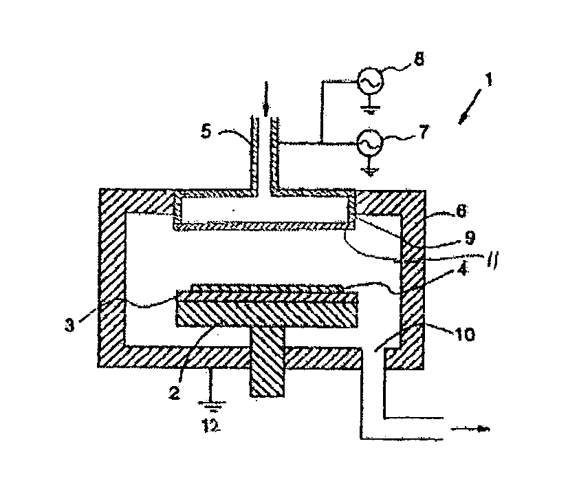
[0034] In the example, the capacitively-coupled plasma CVD apparatus (Eagle®-12 by ASM Japan K. K.) shown in FIG. 1 was used.

[0035] Film Forrming Conditions Used in Example

[0036] A parameter test was conducted under the following conditions:

[0037] Organosilicon Oxide Film

[0038] Silicon source gas: TEOS (60 to 80 sccm)

[0039] Oxidizing gas: O2 (1,400 to 2,600 sccm)

[0040] Inactive gas: He (300 to 1,000 sccm)

[0041] Total pressure: (350 to 450 Pa)

[0042] Substrate temperature: (200° C.)

[0043] Interior wall temperature: (120° C.)

[0044] Showerhead temperature: (100° C.)

[0045] Inter-electrode distance: 10 mm

[0046] First RF power supply (H-RF): 13.56 MHz (0.13 to 0.27 W / cm2)

[0047] Second RF power supply (L-RF): 430 kHz (0.44 to 0.58 W / cm2)

[0048] Substrate: ø300-mm silicon substrate

[0049] Organosilicon oxide film: 2 reference film thicknesses of 100 nm and 400 nm

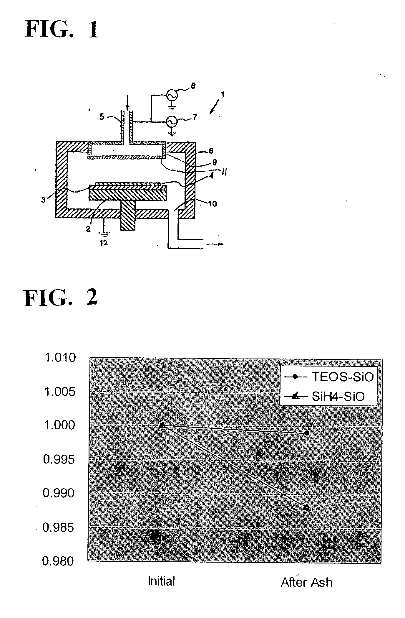
[0050] Evaluation Items

[0051] Refractive index (−), film formation speed (nm), film thickness distribution (±%), str...


PUM

PropertyMeasurementUnit
temperatureaaaaaaaaaa
frequencyaaaaaaaaaa
frequencyaaaaaaaaaa

Abstract

A method of forming an organosilicon oxide film by plasma CVD includes: (i) adjusting a temperature of a susceptor on which a substrate is placed to lower than 300° C.; (ii) introducing at least tetraethylorthosilicate (TEOS) and oxygen into a reactor in which the susceptor is disposed; (iii) applying high-frequency RF power and low-frequency RF power; and (iv) thereby depositing an organosilicon oxide film on the substrate.

Description

CROSS-REFERENCE TO RELATED APPLICATIONS [0001] This is a continuation-in-part application of U.S. patent application Ser. No. 11 / 303,101, filed Dec. 16, 2005, the disclosure of which is incorporated herein by reference in its entirety.BACKGROUND OF THE INVENTION [0002] 1. Field of the Invention [0003] The present invention relates to a semiconductor forming technology by plasma CVD (such as capacitively-coupled CVD), and more specifically to a method of forming a minute low-temperature oxide film and a multilayer resist method utilizing the same with respect to a substrate containing thermally unstable substances. [0004] 2. Description of the Related Art [0005] Integrated semiconductor circuits have become increasingly minute to achieve higher speed and functionality. To produce minute circuits, demands for photolithography, dry-etching and other minute processing technologies are growing stronger. Applications utilizing the multilayer resist method are expanding to address the tren...

Claims


Application Information

Patent Timeline
Patent Type & Authority Applications(United States)
IPC IPC(8): H05H1/24
CPCC23C16/401C23C16/5096H01J37/32091H01J2237/2001H01L21/02126H01L21/02274H01L21/31633
Inventor NAKANO, RYU
Owner ASM JAPAN
Why Eureka
Try Eureka