Electronic part mounting method

a technology for mounting methods and electronic parts, applied in the field of electronic part mounting methods, can solve the problems of insufficient long curing time of resin, and thermal damage of the electronic part, and achieve the effect of shortening the time necessary for joining, enhancing the reliability of the joining portion, and avoiding thermal damag

Inactive Publication Date: 2007-07-05
FUJI ELECTRIC HLDG CO LTD
View PDF4 Cites 18 Cited by
  • Summary
  • Abstract
  • Description
  • Claims
  • Application Information

AI Technical Summary

Benefits of technology

[0025] Further, in the present invention, it is preferable that the surfaces of the above-mentioned circuit electrode and the above-mentioned die electrode are formed of coarse surfaces having the surface roughness Ra of 0.4 to 10 μm, and the above-mentioned coarse surfaces are plastically deformed at the time of joining to enable the joining of the circuit electrode and the die electrode. Due to such a constitution, the electrode surfaces are pressurized until the electrode surfaces are plastically deformed and hence, even when the electrodes which are formed by electrolytic rating or the like, for example have irregularities on surfaces thereof attributed to precipitation, it is possible to obtain a favorable joining state.
[0026] Further, in the present invention, it is preferable that in the above-mentioned heating and pressurizing, the low-melting-point metal layer is maintained under the heating and pressurizing for a predetermined time until the low-melting-metal is completely diffused in the above-mentioned circuit electrode and the die electrode by solid-liquid diffusion. Due to such a constitution, the low-melting-point metal is completely diffused by solid-liquid diffusion thus-forming one alloy layer as a whole. That is, different from soldering, the alloy layer includes no intermediate layer at the joining portion. Accordingly, the reliability of the joining portion does not depend on the characteristic of the interposed joining material but mainly depends on the base metal of the electrode and hence, the reliability of the joining portion further enhanced.
[0027] Further, in the present invention, it is preferable that the above-mentioned low-melting-point metal layer is maintained under the above-mentioned heating and pressurizing for a predetermined time until an intermediate alloy layer is formed between the above-mentioned circuit electrode and the above-mentioned die electrode. Due to such a constitution, the low-melting-point metal is not completely diffused and it is sufficient to perform heating until the intermediate alloy layer is formed whereby it is possible to largely shorten time necessary for joining. Further, a supply quantity of the low-melting-point metal is enough so long as a quantity of low-melting-metal which is necessary for forming the intermediate alloy layer is supplied and hence, a strict management of the supply quantity of the low-melting-metal becomes no more necessary.
[0028] Further, in the present invention, it is preferable that the above-mentioned low-melting-point metal layer is formed such that at least two kinks of metals which can form alloy are stacked in two layers or more, and the stacked metal layers are preheated to make the metal layers react with each other to form an alloy layer. Doe to such a constitution, irregularities of the alloy composition or the supply quantity in the alloy layer can be eliminated and hence, it is possible to realize the stable diffusion joining at the low temperature thus acquiring the high reliable joining portion.
[0029] Further, in the present invention, it is preferable that the above-mentioned low-melting-point metal layer is formed by vapor-depositing alloy which constitutes an evaporation source and, at the time of performing the above-mentioned vapor deposition, an evaporation pressure ratio in reaction steps of respective components of the above-mentioned alloy is controlled thus forming a film having the target alloy composition. Due to such a constitution, it is possible to perform the control of the composition of the alloy at the time of vapor deposition and hence, it is possible to turn the alloy composition of the low-melting-point metal layer into the eutectic composition which enables the joining at a lowermost temperature thus ensuring the stable diffusion joining at the low temperature. Further, with the use of the vapor deposition method, it is possible to easily form the film having the thickness which allows the easy diffusion of the low-melting-point metal layer by the vapor deposition method.
[0030] Further, in the present invention, it is preferable that the-above-mentioned low-melting-point metal layer-is formed by vapor-depositing alloy which constitutes an evaporation source and, at the time of performing the above-mentioned vapor deposition, a product of an evaporation pressure ratio and an active coefficient ratio in reaction steps of respective components of the above-mentioned alloy is controlled thus forming a film having the target alloy composition. Due to such a constitution, it is possible to perform the control of the composition of the alloy at the time of vapor deposition and hence, it is possible to turn the alloy composition of the low-melting-point metal layer into the eutectic composition which enables the joining at a lowermost temperature thus ensuring the stable diffusion joining at the low temperature. Further, with the use of the vapor deposition method, it is possible to easily form the film having the thickness which allows the easy diffusion of the low-melting-point metal layer by the vapor deposition method.

Problems solved by technology

In this case, a heating temperature at the time of joining, when the joining is performed by soldering, depends on a melting point of a solder material and hence, a high temperature of 200 to 300° C. is required in usual soldering thus giving rise to a drawback that an electronic part is thermally damaged.
Further, when the resin adhesive agent is used, although a heating temperature is at a low temperature of 150 to 200° C., there arises a drawback that the curing of resin requires a long time of 30 to 60 minutes.
However, when the above-mentioned solder or resin adhesive agent is used as the joining material, these materials have drawbacks with respect to the high-temperature property and the thermal fatigue lifetime thus giving rise to a drawback that the joining portion cannot obtain the sufficient reliability.
Further, in performing the solder joining, it is necessary to supply a large quantity of solder with a usual thickness of 15 μm or more and hence, it is necessary to ensure a joining distance of 300 μm or more thus making the finer joining difficult.
Further, also in performing the joining using the resin adhesive agent, to satisfy the insulating property and the connection resistance, it is usually necessary to ensure a joining distance of 100 μm or more thus making the fine joining with the joining distance of less than 100 μm difficult.
Further, in the method for forming the lead-free solder bumps disclosed in JP-A-2002-43348, the joining at a low temperature for a short time is insufficient.
For example, the joining at a low temperature of 200° C. or less and for a short time is difficult.
Further, in the alloy vapor deposition method of the JP-A-5-9713, it is necessary to obtain the relationship between the composition of the base alloy in the crucible and the alloy composition in the vapor-deposited film and, it is necessary to determine the composition of the base alloy based on a correction curve thus giving rise to a drawback that the preparation steps up to the vapor deposition becomes cumbersome.

Method used


Image

  • Electronic part mounting method
  • Electronic part mounting method
  • Electronic part mounting method

Examples


example 1

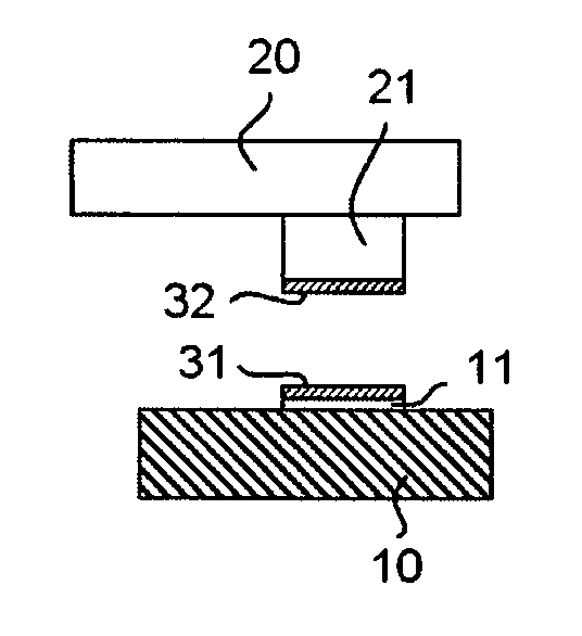
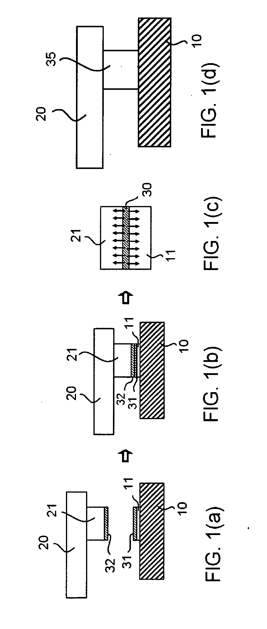
[0116] An electronic part is mounted on a circuit board using the method shown in FIG. 1.

[0117] First of all, a semiconductor chip is used as the electronic part, and bumps made of Cu are formed over the semiconductor chip as electrodes. On the other hand, Cu electrodes are formed over the circuit board.

[0118] Next, as a low-melting-point metal layer, over the Cu bump of the semiconductor chip and over the Cu electrode of the circuit board, an SnIn layer (melting point: 117° C.) having a total thickness of 4 μm, wherein an Sn layer has a thickness of 2 μm and In layer having a thickness of 2 μm is formed by vapor deposition.

[0119] Here, in a vapor deposition method, mother alloy made of SnIn (In:Sn=52:48) is used as an evaporation source, and a film is formed by controlling a vapor deposition condition such that the vapor pressure ratio (PA / PB)=0.81 in the above-mentioned formula (12) becomes (PA / PB)=0.81. Here, an electron beam vapor deposition apparatus is used as a vapor depos...

embodiment 2

[0123] The joining of a semiconductor chip and a circuit board is performed under the same condition as the embodiment 1 except for that, in the formation of a low-melting-point metal layer vapor deposition, a film is formed by controlling a product of a vapor pressure ratio and an activity constant ratio (γAPA / γBPB)=0.98 in the above-mentioned formula (16) becomes (γAPA / γBPB)=0.98.

[0124] As a result, the composition of the formed SnIn thin film is set to In:Sn=52:48 and hence, the low-melting-point metal layer having the target alloy composition is obtained. Further, after joining, as shown in FIG. 1(d), it is confirmed by a cross-section observation using a high vacuum scanning electron microscope and an element analysis of a joining interface by an X-ray micro analyzer (EPMA) that SnIn is completely diffused in the Cu electrode and the joining portion which constitutes one alloy layer as a whole in which an intermediate alloy layer is not present is obtained.

example 3

[0125] An electronic part is mounted on a circuit board using the method shown in FIG. 1.

[0126] First of all, a semiconductor chip is used as the electronic part, and bumps made of Cu are formed over the semiconductor chip as electrodes. On the other hand, Cu electrodes are formed over the circuit board.

[0127] Next, as a low-melting-point metal layer, over the Cu bump of the semiconductor chip and over the Cu electrode of the circuit board, an Sn layer having a thickness of 0.48 μm and an In layer having a thickness of 0.52 μm are sequentially formed as a single metal layer by vapor deposition such that a total thickness becomes 1 μm.

[0128] Then, as shown in FIG. 1(a), the Cu bump of the semiconductor chip and the Cu electrode of the circuit board are aligned with each other and, thereafter, as shown in FIG. 1(b), the electrodes are brought into contact with each other. Then, preheating is performed at a temperature of 120° C. for 10 seconds so as to form the Sn layer and the In ...


PUM

PropertyMeasurementUnit
temperatureaaaaaaaaaa
surface roughness Raaaaaaaaaaa
temperatureaaaaaaaaaa

Abstract

The present invention provides an electronic part mounting method which enables joining of electrodes at a low temperature and within a short time, can obtain the high reliability and, further, enables joining at a fine pitch. In an electronic part mounting method which joins circuit electrodes which are formed over a circuit board and die electrodes which are formed over the electronic parts thus mounting the electronic parts on the circuit board, a low-melting-point metal layer is preliminarily formed over the circuit electrode and/or the die electrode and, thereafter, the circuit electrode and the die electrode are arranged to face each other and are heated and pressurized for melting low-melting-point metal thus diffusing the low-melting-point metal into the circuit electrode and the die electrode by solid-liquid diffusion.

Description

TECHNICAL FIELD [0001] The present invention relates to, for example, a method which, in a circuit board or a module (multiple chip module) or the like which requires the miniaturization, directly mounts electronic parts such as semiconductor chips on the circuit board such as a printed circuit board. BACKGROUND ART [0002] Along with the miniaturization or the sophistication of functions of electronic equipments in recent years, a mounting method which directly mounts electronic parts such as semiconductor chips directly on a circuit board, so-called bare chip mounting, has been popularly put into practice. [0003] In FIG. 3(a), (b), one example of the bare chip mounting which has been performed conventionally is shown. [0004] In FIG. 3(a), a circuit board electrode 51 which is formed over a substrate 50 and a bump (electrode) 61 made of Au or solder which is formed over a semiconductor chip 60 by way of an electrode pad 62 are brought into contact with each other in an opposed manne...

Claims


Application Information

Patent Timeline
Patent Type & Authority Applications(United States)
IPC IPC(8): B23K31/02H01L21/60H05K3/32
CPCH01L24/12H01L24/16H01L2924/07811H01L24/81H01L2224/13099H01L2224/13147H01L2224/16H01L2224/81193H01L2224/81204H01L2924/01013H01L2924/01015H01L2924/01029H01L2924/01032H01L2924/01033H01L2924/01051H01L2924/01078H01L2924/01079H01L2924/01082H01L2924/01088H01L2924/01322H05K3/328H05K2203/0278H01L2224/81825H01L2924/01005H01L2924/01006H01L2924/01019H01L2924/01047H01L2924/0105H01L2924/014H01L2924/00H01L2224/05573H01L2224/05568H01L2224/05624H01L2224/05644H01L2224/05647H01L2224/05655H01L2924/00014H01L2224/0554H01L24/05H01L24/13H01L2224/05599H01L2224/0555H01L2224/0556
Inventor FUJIMOTO, KOZOIKEMI, KAZUTAKAWATANABE, HIROHIKOMATSUMURA, KEIICHISHIMODA, MASAYOSHITANIGUCHI, KATSUMIGOTO, TOMOAKI
Owner FUJI ELECTRIC HLDG CO LTD
Why Eureka
Try Eureka