
Purification process for organic electronics material

a technology of organic electronics and purification process, which is applied in the direction of discharge tube luminescence screen, separation process, liquid cleaning, etc., can solve the problems of easy degradation of luminescence efficiency, low efficiency, and low stability, and achieve the effect of effective removal

Active Publication Date: 2007-07-12
MAXDEM +1
View PDF8 Cites 12 Cited by
  • Summary
  • Abstract
  • Description
  • Claims
  • Application Information

AI Technical Summary

Problems solved by technology

When the Pd remains in the material, problems in terms of luminescence characteristics such as an increase in the luminescence starting voltage, a degradation in the luminescence efficiency, and a degradation in the stability easily occur.
However, it is difficult to remove Pd by these methods.

Method used


Image

  • Purification process for organic electronics material
  • Purification process for organic electronics material
  • Purification process for organic electronics material

Examples


examples

[0040] The present invention is explained further in detail below with reference to Examples, but the present invention is not limited by the Examples below.

synthetic examples 1 and 2

Synthesis of Polymer

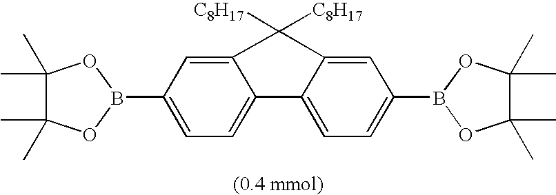
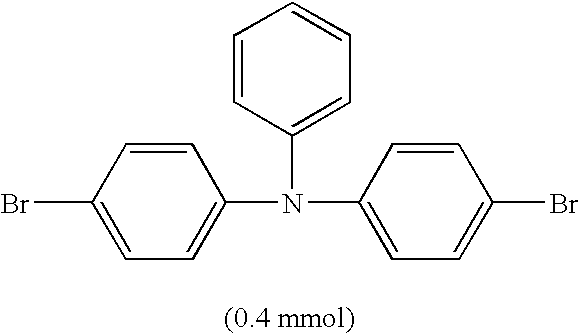
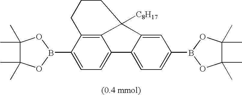
[0041] A reaction was carried out using a dedicated polytetrafluoroethylene reaction vessel. With regard to a solvent, oxygen in the solvent was removed using nitrogen gas for 30 minutes or longer before use. The reaction vessel was charged with monomers shown in Table 1 and further, in a glove box under an atmosphere of nitrogen, with a 3 vol % anisole solution (8 ml) of tricaprylmethylammonium chloride and an 8 mM anisole solution (100 μL) of Pd(PPh3)4. After the monomers were dissolved by stirring, a 2M aqueous solution (5.3 ml) of K2CO3 was added. The reaction vessel was set in a microwave reaction device, and a Suzuki coupling reaction was carried out while stirring under microwave irradiation with conditions shown in Table 2. As a reference for controlling the temperature, a mixture of all the reagents and solvents other than the monomers was used. After the reaction was completed, the reaction mixture was poured into methanol-water (ratio by volume (the sa...

examples 1 and 2

Purification of Polymer

[0046] The polymer obtained in Synthetic Examples 1 and 2 was dissolved in toluene (10 ml relative to 100 mg of polymer), triphenylphosphine, polymer-bound on styrene-divinylbenzene copolymer (200 mg relative to 100 mg of polymer, 15-6730, manufactured by STREM Chemicals Inc.) was added, and stirring was carried out overnight. After stirring was completed, the triphenylphosphine, polymer-bound on styrene-divinylbenzene copolymer was removed by filtration, and the filtrate was concentrated using a rotary evaporator. The residue was dissolved in toluene, and then reprecipitated from methanol-acetone (8:3). The precipitate thus formed was filtered by suction and washed with methanol-acetone (8:3). The precipitate thus obtained was dried in vacuum to give a polymer. The polymer thus obtained was subjected to ICP emission analysis, and the results are given in Table 4.

TABLE 4Crude polymerproductPd content (ppm)Example 3Synthetic Example 1Example 4Synthetic Exam...


PUM

PropertyMeasurementUnit
temperatureaaaaaaaaaa

Abstract

Objects of the present invention are to provide a purification process that enables Pd contained in an organic electronics material to be removed effectively, to provide an electroluminescent device middle layer material purified by the process, and to provide an electroluminescent device employing the middle layer material. The present invention relates to a process for purifying an organic electronics material, the process involving treating, with a phosphorus-containing material, an organic electronics material that contains Pd as an impurity so as to remove the Pd.

Description

BACKGROUND OF THE INVENTION [0001] 1. Field of the Invention [0002] The present invention relates to a purification process for an organic electronics material, an electroluminescent device middle layer material purified by the process, and an electroluminescent device employing the middle layer material. [0003] 2. Description of the Related Art [0004] Electroluminescent devices have been attracting attention as, for example, large-area solid state light sources to replace incandescent lamps and gas-filled lamps. They have also been attracting attention as self-luminous displays, and are the most promising alternative to liquid crystal displays in the flat panel display (FPD) field. In particular, an organic electroluminescent (EL) device, in which the device material is formed from an organic material, is being commercialized as a low power consumption full-color FPD. Above all, polymer-based organic EL devices will be indispensable for future large-screen organic EL displays since...

Claims


Application Information

Patent Timeline
Patent Type & Authority Applications(United States)
IPC IPC(8): B08B7/04B08B7/00H01L51/00H10K99/00
CPCH01L51/0025H01L51/0036H01L51/56H01L51/0043H01L51/0059H01L51/0039H10K71/311H10K85/113H10K85/115H10K85/151H10K85/631H10K71/40H10K71/00
Inventor TSUDA, YOSHIHIROMORISHITA, YOSHIINOMURA, SATOYUKIHOSHI, YOUSUKEFUNYUU, SHIGEAKIMOTAMEDI, FARSHAD J.WANG, LI-SHENG
Owner MAXDEM
Learn More