
Automatic layer deposition process

a layer deposition process and automatic technology, applied in chemical vapor deposition coatings, coatings, capacitors, etc., can solve the problems of only achieving complete coverage of the surface in the trench region, unacceptably long time, etc., to achieve low vapour pressure, reduce effective sticking coefficient, and high sticking coefficient

Inactive Publication Date: 2007-07-12
INFINEON TECH AG
View PDF7 Cites 2 Cited by
  • Summary
  • Abstract
  • Description
  • Claims
  • Application Information

AI Technical Summary

Benefits of technology

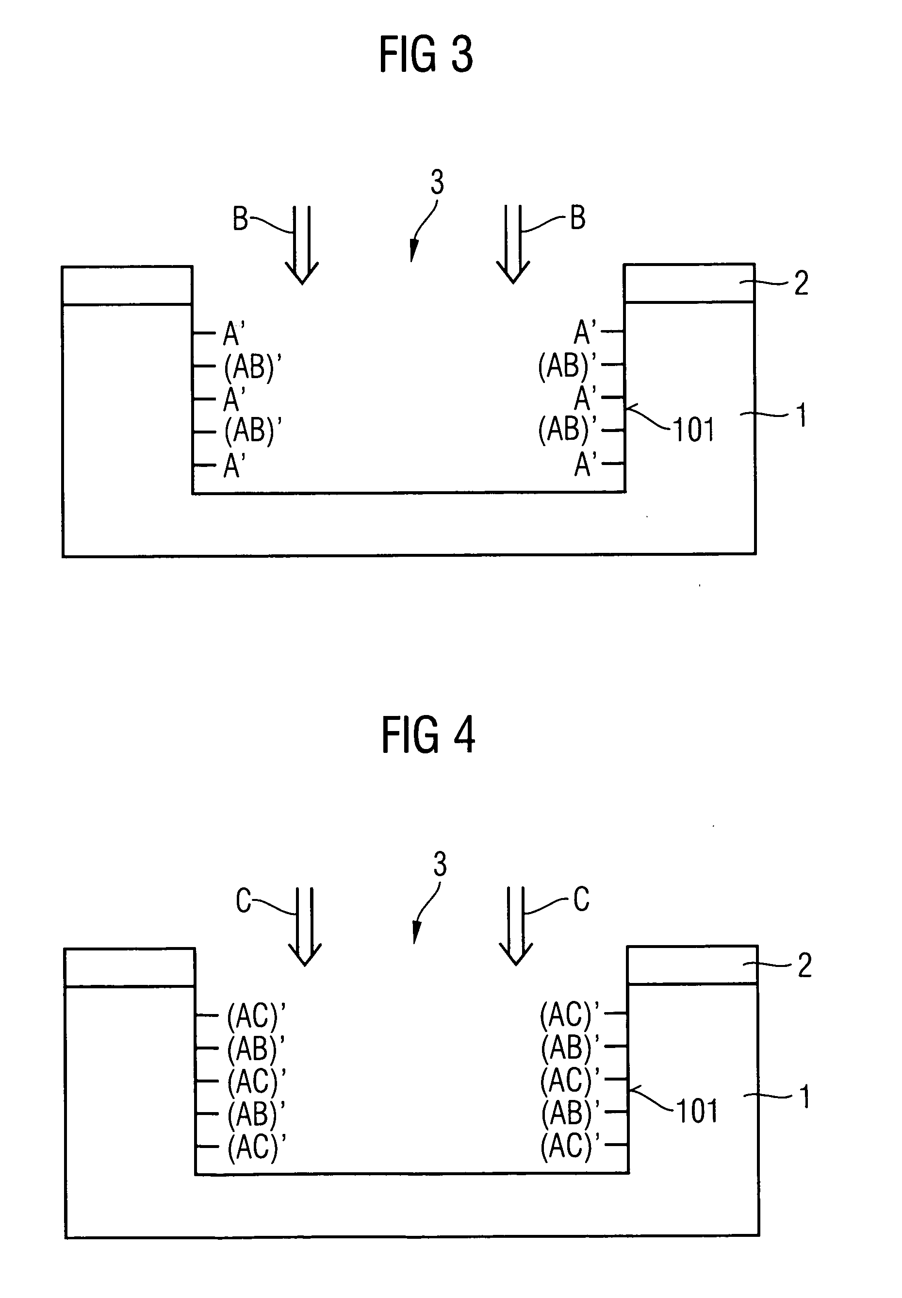
[0012] The second precursor having the low sticking coefficient requires a greater number of contacts with the surface before it reacts with an intermediate product located on the surface. On account of the high number of attempts, the second precursor covers long distances before it reacts. This results in a relatively uniform distribution of the second precursor over the entire surface or of the product of the second precursor with the intermediate product on the surface. The third precursor reacts substantially only with the intermediate product and not with the first product, which results from the intermediate product and the second precursor. If the third precursor comes into contact with the first product, no reaction takes place. The high sticking coefficient of the third precursor is therefore reduced by the partial coverage of the surface with the first product. This results in a more uniform distribution of the third precursor over the surface and of its products with the intermediate product on the surface.
[0014] According to another embodiment, the third precursor includes a metal compound or hafnium and / or zirconium and / or a lanthanide. The process is particularly suitable for metal compounds, since these generally have a high sticking coefficient of greater than 0.1. Precursors which transport hafnium, zirconium and the lanthanides also have a low vapour pressure, resulting in the risk of non-conformal layer deposition as a result of an insufficient quantity of precursor being introduced. In this case, the advantageous effect results from the reduction in the effective sticking coefficient by means of the second precursor. A suitable second precursor may be a silicon compound, e.g. silane. The first precursor may form hydroxyl groups by means of water vapour or ammonium groups by means of ammonia.
[0015] In another embodiment, the undesired first product is released from the surface following the introduction of the third precursor. The voids can be filled by monolayers that are subsequently applied. The releasing of the first product can be achieved by increasing the temperature.

Problems solved by technology

Complete coverage of the surfaces in the region of the trench is only achieved after an in some cases unacceptably long time following the introduction of the precursors.

Method used


Image

  • Automatic layer deposition process
  • Automatic layer deposition process
  • Automatic layer deposition process

Examples


Embodiment Construction

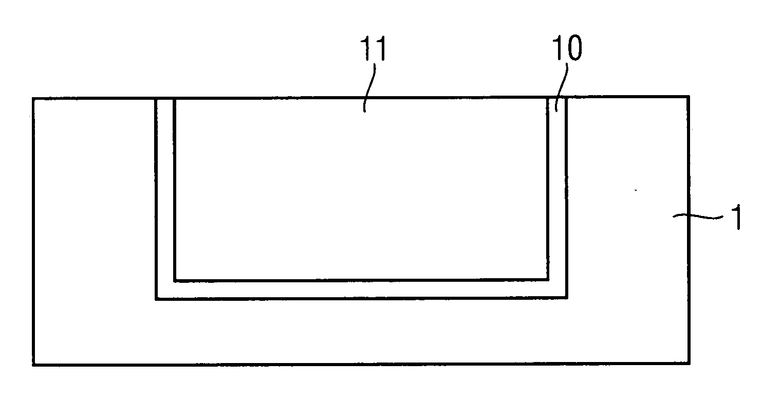
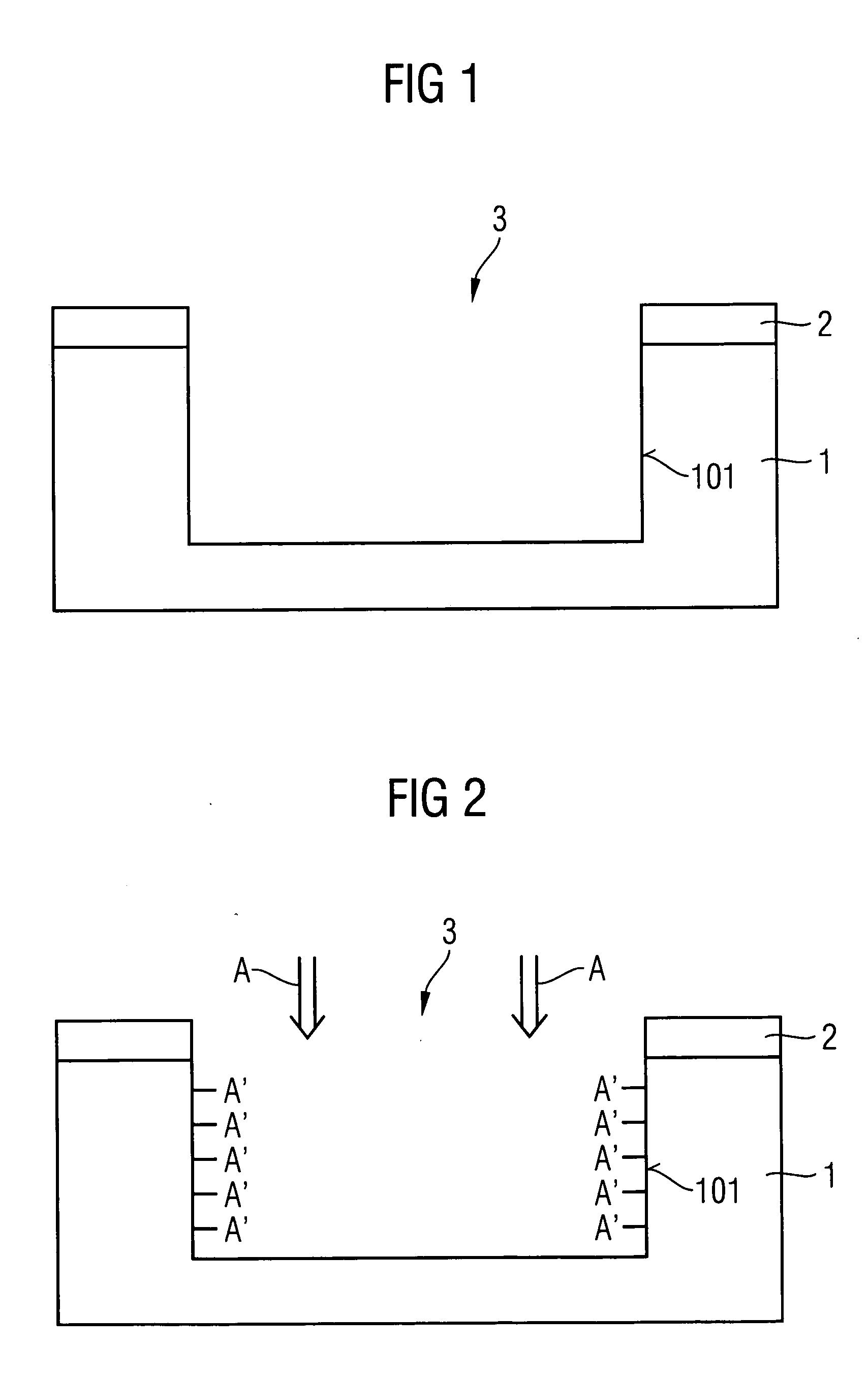
[0022]FIG. 1 illustrates a semiconductor substrate 1, for example made from silicon. A capping layer 2 of silicon oxide, silicon nitride or other passivating materials has been deposited thereon. A trench 3 has been formed through the capping layer 2 and into the substrate 1. Contrary to the geometry illustrated in FIG. 1, this trench may also have a very high aspect ratio, i.e. the depth of the trench is higher by a multiple than the width of the trench. In 90 nanometre technology, trenches with a depth of from 6 to 9 μm and an aspect ratio of 1:80 are typically produced. A thin layer with a thickness of just a few nanometres is to be deposited in the trench. In the text which follows, by way of example, the deposition of a thin layer of a dielectric material is described; however, it is also possible for metal layers with a high conductivity to be deposited in a similar way.

[0023] In a first step, a first reaction gas, referred to below as precursor A, is introduced into a reacti...


PUM

PropertyMeasurementUnit
depthaaaaaaaaaa
depthaaaaaaaaaa
aspect ratioaaaaaaaaaa

Abstract

The atomic layer deposition process according to the invention provides the following steps for the production of homogeneous layers on a substrate. The substrate is introduced into a reaction chamber. A first precursor is introduced into the reaction chamber, which first precursor reacts on the surface of the substrate to form an intermediate product. A second precursor is introduced into the reaction chamber, which second precursor has a low sticking coefficient and reacts with part of the intermediate product to form a first product. A third precursor is introduced into the reaction chamber, which third precursor has a high sticking coefficient and reacts with the remaining part of the intermediate product to form a second product. The second precursor and its first product reduce the effective sticking coefficient of the third precursor by partially covering the surface.

Description

CLAIM FOR PRIORITY [0001] This application claims the benefit of priority to German Application No. 10 2005 062 917.2, filed in the German language on Dec. 29, 2005, the contents of which are hereby incorporated by reference. TECHNICAL FIELD OF THE INVENTION [0002] The present invention relates to an atomic layer deposition process (ALD process) which is suitable for producing a homogeneous layer on a substrate. BACKGROUND OF THE INVENTION [0003] For many applications, capacitors must not drop below a minimum capacitance. The capacitance of a capacitor is dependent, inter alia, on the surface area of the electrode surfaces of the capacitors. Therefore, their surface area must not drop below a minimum value. [0004] There is a requirement for a large number of semiconductor components to be arranged at or on a surface of a semiconductor substrate. This is achieved by reducing the lateral dimensions of the semiconductor components and also of the capacitors. The minimum surface area of...

Claims


Application Information

Patent Timeline
Patent Type & Authority Applications(United States)
IPC IPC(8): H01L21/8242
CPCC23C16/34C23C16/45525H01L28/40H01L21/3141H01L21/318C23C16/45531H01L21/0228H01L21/0217H01L21/02181
Inventor ERBEN, ELKEJAKSCHIK, STEFANKERSCH, ALFREDLINK, ANGELASUNDQVIST, JONAS
Owner INFINEON TECH AG
Learn More