High-throughput printing of semiconductor precursor layer by use of chalcogen-containing vapor and inter-metallic material

Inactive Publication Date: 2007-07-19
AERIS CAPITAL SUSTAINABLE IP
View PDF99 Cites 129 Cited by
  • Summary
  • Abstract
  • Description
  • Claims
  • Application Information

AI Technical Summary

Benefits of technology

[0014] In one embodiment of the present invention, the method comprises forming a precursor material comprising group IB and/or group IIIA and/or group VIA particles of any shape. The method may include forming a precursor layer of the precursor material over a surface of a substrate. The method may further include heating the particle precursor material in a substantially oxygen-free chalcogen atmosphere to a processing temperature sufficient to react the particles and to release chalcogen from the chalcogenide particles, wherein the chalcogen assumes a liquid form and acts as a flux to improve intermixing of elements to form a group IB-IIIA-chalcogenide film at a desired stoichiometric ratio. The suitable atmosphere may be a selenium atmosphere. The suitable atmosphere may comprise of a selenium atmosphere providing a partial pressure greate

Problems solved by technology

These electronic devices have been traditionally fabricated using silicon (Si) as a light-absorbing, semiconducting material in a relatively expensive production process.
A central challenge in cost-effectively constructing a large-area CIGS-based solar cell or module is that the elements of the CIGS layer must be within a narrow stoichiometric ratio on nano-, meso-, and macroscopic length scale in all three dimensions in order for the resulting cell or module to be highly efficient.
Achieving precise stoichiometric composition over relatively large substrate areas is, however, difficult using traditional vacuum-based deposition processes.
For example, it is difficult to deposit compounds and/or alloys containing more than one element by sputtering or evaporation.
Both techniques rely on deposition approaches that are limited to line-of-sight and limited-area sources, tending to result in poor surface coverage.
Line-of-sight trajectories and limited-area sources can result in non-uniform distribution of the elements in all three dimensions and/or poor film-thickness uniformity over large areas.
Such non-uniformity also alters the local stoichiometric ratios of the absorber layer, decreasing the potential power conversion efficiency of the complete cell or module.
However, solar cells fabricated from the sintered layers had very low efficiencies because the structural and electronic quality of these absorbers was poor.
A difficulty in this approach was finding an appropriate fluxing agent for dense CuInSe2 film formation.
So far, no promising results have been obtained when using chalcogenide powders for fast processing to form CIGS thin-films suitable for solar cells.
Due to high temperatures and/or long processing times required for 
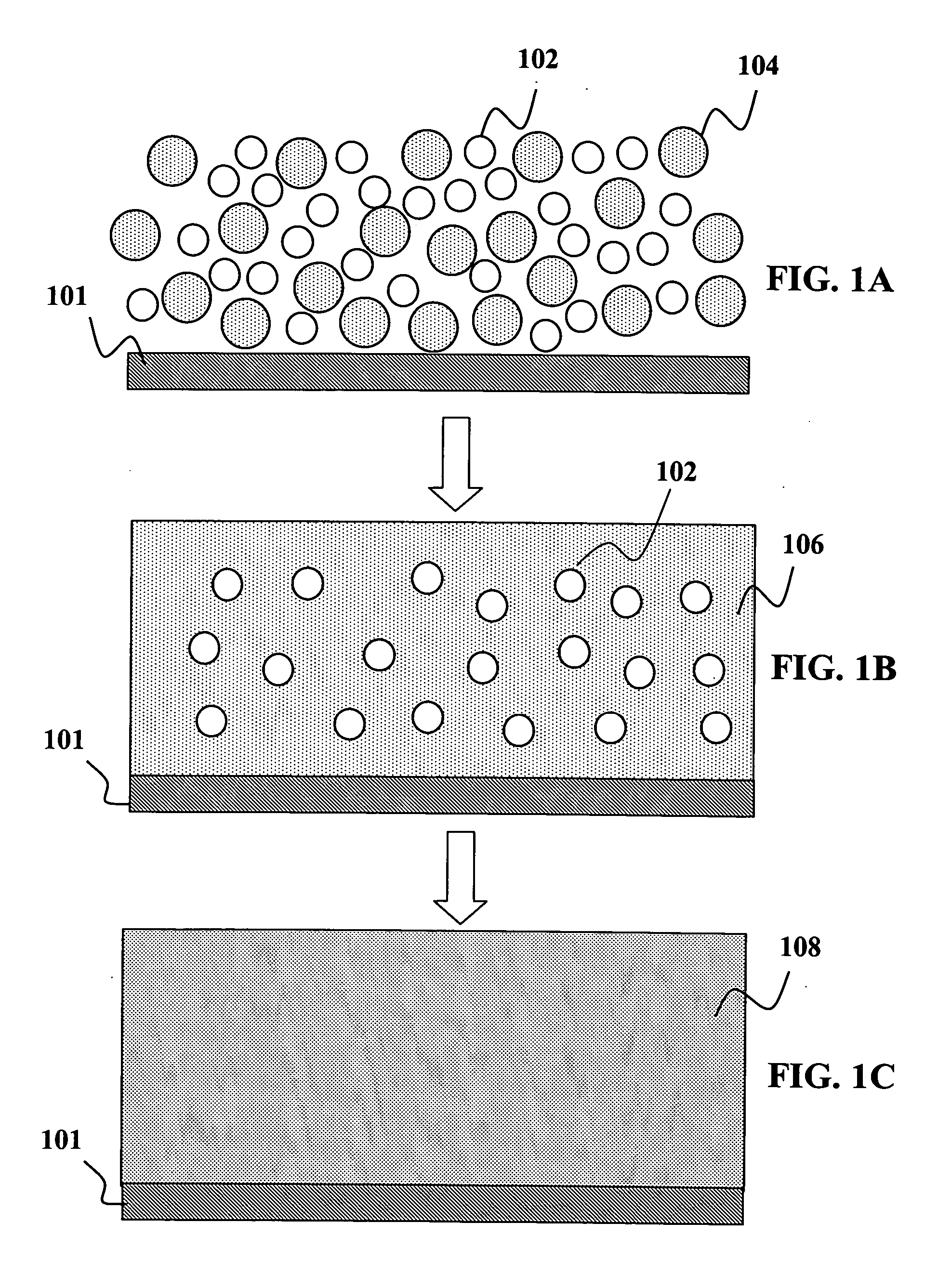
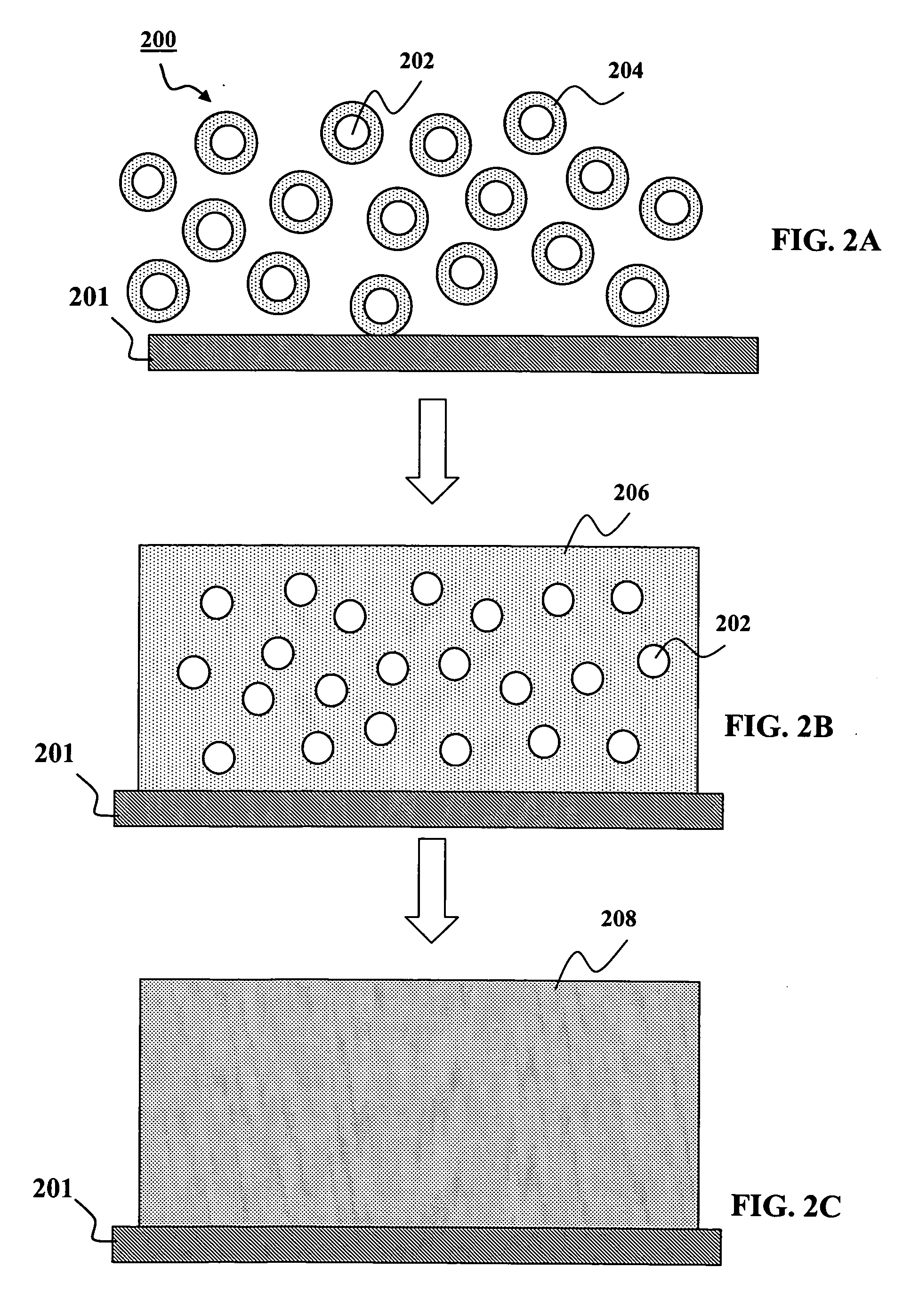
sintering, formation of a IB-IIIA-chalcogenide compound film suitable for thin-film solar cells is challenging when start

Method used


Image

  • High-throughput printing of semiconductor precursor layer by use of chalcogen-containing vapor and inter-metallic material
  • High-throughput printing of semiconductor precursor layer by use of chalcogen-containing vapor and inter-metallic material
  • High-throughput printing of semiconductor precursor layer by use of chalcogen-containing vapor and inter-metallic material

Examples


Embodiment Construction

[0050] It is to be understood that both the foregoing general description and the following detailed description are exemplary and explanatory only and are not restrictive of the invention, as claimed. It may be noted that, as used in the specification and the appended claims, the singular forms “a”, “an” and “the” include plural referents unless the context clearly dictates otherwise. Thus, for example, reference to “a material” may include mixtures of materials, reference to “a compound” may include multiple compounds, and the like. References cited herein are hereby incorporated by reference in their entirety, except to the extent that they conflict with teachings explicitly set forth in this specification.

[0051] In this specification and in the claims which follow, reference will be made to a number of terms which shall be defined to have the following meanings:

[0052]“Optional” or “optionally” means that the subsequently described circumstance may or may not occur, so that the...


PUM

PropertyMeasurementUnit
Fractionaaaaaaaaaa
Fractionaaaaaaaaaa
Fractionaaaaaaaaaa

Abstract

A high-throughput method of forming a semiconductor precursor layer by use of a chalcogen-containing vapor is disclosed. In one embodiment, the method comprises forming a precursor material comprising group IB and/or group IIIA particles of any shape. The method may include forming a precursor layer of the precursor material over a surface of a substrate. The method may further include heating the particle precursor material in a substantially oxygen-free chalcogen atmosphere to a processing temperature sufficient to react the particles and to release chalcogen from the chalcogenide particles, wherein the chalcogen assumes a liquid form and acts as a flux to improve intermixing of elements to form a group IB-IIIA-chalcogenide film at a desired stoichiometric ratio. The chalcogen atmosphere may provide a partial pressure greater than or equal to the vapor pressure of liquid chalcogen in the precursor layer at the processing temperature.

Description

CROSS-REFERENCE TO RELATED APPLICATION [0001] This application is a continuation-in-part of commonly-assigned, co-pending application Ser. No. 11 / 243,522 entitled “HIGH-THROUGHPUT PRINTING OF CHALCOGEN LAYER” filed Feb. 23, 2006, which is a continuation-in-part of commonly-assigned, co-pending application Ser. No. 11 / 290,633 entitled “CHALCOGENIDE SOLAR CELLS” filed Nov. 29, 2005 and Ser. No. 10 / 782,017, entitled “SOLUTION-BASED FABRICATION OF PHOTOVOLTAIC CELL” filed Feb. 19, 2004 and published as U.S. patent application publication 20050183767. This application is also a continuation-in-part of commonly-assigned, co-pending U.S. patent application Ser. No. 10 / 943,657, entitled “COATED NANOPARTICLES AND QUANTUM DOTS FOR SOLUTION-BASED FABRICATION OF PHOTOVOLTAIC CELLS” filed Sep. 18, 2004. This application is a also continuation-in-part of commonly-assigned, co-pending U.S. patent application Ser. No. 11 / 081,163, entitled “METALLIC DISPERSION”, filed Mar. 16, 2005. This application...

Claims


Application Information

Patent Timeline
IPC IPC(8): B05D3/00
CPCC23C18/1204H01L31/02008H01L31/0322Y02E10/541H01L31/0749H01L31/18H01L31/048
Inventor VAN DUREN, JEROEN K. J.ROBINSON, MATTHEW R.SAGER, BRIAN M.
Owner AERIS CAPITAL SUSTAINABLE IP
Why Eureka
Try Eureka