Electrically rewritable non-volatile memory element and method of manufacturing the same

a non-volatile memory element, electric rewritability technology, applied in the direction of digital storage, instruments, semiconductor devices, etc., can solve the problems of reducing the electrical power consumption of the device, dram is volatile memory that loses stored data, and the limit of the device electrical power consumption can be reduced, so as to improve the heating efficiency and reduce the write current. , the effect of high heating efficiency

Active Publication Date: 2007-07-19
MICRON TECH INC
View PDF9 Cites 22 Cited by
  • Summary
  • Abstract
  • Description
  • Claims
  • Application Information

AI Technical Summary

Benefits of technology

[0021] By thus providing a structure consisting of a block layer between the recording layer and the top electrode, a non-volatile memory element having high heating efficiency can be manufactured.
[0022] In this case too, it is preferable for the block layer to be constituted of phase change material having a composition that differs from that of the phase change material constituting the recording layer, and for the phase change material of the block layer to have a crystallization temperature that is higher than th

Problems solved by technology

DRAM is volatile memory that loses stored data if its power supply is turned off.
That makes DRAM unsuitable for the storage of programs and archival information.
Also, even when the power supply is turned on, the device has to periodically perform refresh operations in order to retain stored data, so there are limits as to how much device electrical power consumption can be reduced, while yet a further problem is the complexity of the controls run under the controller.
Semiconductor flash memory is high capacity and non-volatile, but requires high current for writing and erasing data, and write and eras

Method used


Image

  • Electrically rewritable non-volatile memory element and method of manufacturing the same
  • Electrically rewritable non-volatile memory element and method of manufacturing the same
  • Electrically rewritable non-volatile memory element and method of manufacturing the same

Examples


first embodiment

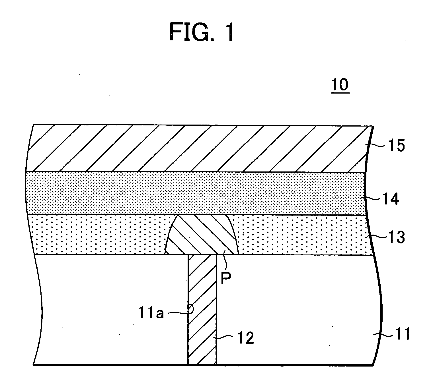
[0037]FIG. 1 is a cross-sectional view of the memory element according to the present invention.

[0038] As shown in FIG. 1, the non-volatile memory element 10 according to this embodiment includes an interlayer isolation layer 11, a bottom electrode 12 buried within the interlayer isolation layer 11, and a recording layer 13, block layer 14 and top electrode 15 formed, in that order, on the interlayer isolation layer 11. In this embodiment, the top electrode 15 is also used as a bit line.

[0039] The interlayer isolation layer 11 can be formed of silicon oxide or silicon nitride or the like. The bottom electrode 12 is formed in a through-hole 11a formed in the interlayer isolation layer 11.

[0040] The bottom electrode 12 is used as a heater plug. That is, it constitutes part of the heater during data writes. For this, the bottom electrode 12 is preferably formed of a material having a relatively high electrical resistance, such as metal silicides, metal nitrides and nitrides of metal ...

second embodiment

[0080] Next, a non-volatile memory element 20 according to the present invention is described.

[0081]FIG. 10 is a drawing showing the cross-section of the memory element 20 according to the second embodiment of the present invention.

[0082] As shown in FIG. 10, the memory element 20 differs from the memory element 10 in having an intermediate layer 21 between the recording layer 13 and the block layer 14. Other parts and elements are the same and are denoted by the same reference numerals, so repeated explanation thereof is omitted.

[0083] The intermediate layer 21 serves to prevent intermixing between the recording layer 13 and the block layer 14. There is no particular limitation on the material of the intermediate layer 21, as long as it can prevent the recording layer 13 and block layer 14 from intermixing. However, it is preferable to choose a material having a higher electrical resistance than the recording layer 13. If the electrical resistance of the intermediate layer 21 is ...


PUM


Abstract

A non-volatile memory element comprises a bottom electrode 12; a top electrode 15; and a recording layer 13 containing phase change material and a block layer 14 that can block phase change of the recording layer 13, provided between the bottom electrode 12 and the top electrode 15. The block layer 14 is constituted of material having an electrical resistance that is higher than that of material constituting the recording layer 13. The block layer 14 suppresses the radiation of heat towards the top electrode 15 and greatly limits the phase change region when a write current is applied. The result is a high heating efficiency. The top electrode 15 itself can be used to constitute a bit line, or a separate bit line can be provided.

Description

TECHNICAL FIELD [0001] The present invention relates to an electrically rewritable non-volatile memory element and to a method of manufacturing the element. More specifically, the present invention relates to an electrically rewritable non-volatile memory element having a recording layer that includes phase change material, and to a method of manufacturing the element. BACKGROUND OF THE INVENTION [0002] Personal computers and servers and the like use a hierarchy of memory devices. There is lower-tier memory, which is inexpensive and provides high storage capacity, while memory higher up the hierarchy provides high-speed operation. The bottom tier generally consists of magnetic storage such as hard disks and magnetic tape. In addition to being non-volatile, magnetic storage is an inexpensive way of storing much larger quantities of information than solid-state devices such as semiconductor memory. However, semiconductor memory is much faster and can access stored data randomly, in co...

Claims


Application Information

Patent Timeline
IPC IPC(8): H01L29/06H01L21/00
CPCH01L45/06H01L45/1233H01L27/2436H01L45/144H01L45/1625H01L45/126G11C13/0004G11C13/0069G11C2213/79H10B63/30H10N70/231H10N70/8413H10N70/826H10N70/8828H10N70/026
Inventor ASANO, ISAMUSATO, NATSUKICZUBATYJ, WOLODYMYRFOURNIER, JEFFREY P.
Owner MICRON TECH INC
Why Eureka
Try Eureka