Semiconductor laser device and laser projector

a laser device and semiconductor technology, applied in semiconductor lasers, laser optical resonator construction, laser details, etc., can solve the problems of inability to accurately reproduce brightness, color, contrast, and large change in transverse mode oscillation shape, and achieve high threshold carrier density and differential gain high

Active Publication Date: 2007-07-19
PANASONIC CORP
View PDF16 Cites 51 Cited by
  • Summary
  • Abstract
  • Description
  • Claims
  • Application Information

AI Technical Summary

Benefits of technology

[0067] According to the present invention, in the semiconductor laser device having different reflectivities at the both facets of the resonator, the electrode disposed on the stripe structure for injecting carriers into the active layer is divided into plural parts, and driving voltages are applied to the respective electrode parts so that the carrier density distribution within the active layer becomes a distribution according to the light intensity distribution in the resonator direction, whereby occurrence of a region where the injection carrier density is excessively high is suppressed, resulting in a semiconductor laser device which can perform laser oscillation with a stable transverse mode.
[0068] Further, in the present invention, since the stripe structure is tapered, it is possible to resolve shortage of injection carriers at the light emission facet side of the resonator where the light intensity is high, and ease the phenomenon that the carrier density in the active layer becomes extremely high in the vicinity of the rear facet of the resonator where the light intensity is low. The increase in the light output power by making the stripe structure have the taper shape is particularly effective in a gallium nitride system semiconductor laser having a high threshold carrier density and a high differential gain.

Problems solved by technology

However, when the carrier density inside the active layer is too high, saturation of the light output occurs due to gain saturation caused by spatial hole burning, whereby the high output operation is impeded.
In addition, in the wide-stripe laser, although no kink occurs since the transverse mode of the waveguide light is a multimode, the shape of the transverse mode oscillation greatly changes to be unstable due to the spatial gain saturation caused by spatial hole burning.
Further, in a light source for a laser display, although the light condensing characteristic up to the diffraction limit is not required as described above, when the transverse mode changes at a low frequency, the brightness of the display changes temporally, resulting in a problem that the brightness, color, and contrast cannot be accurately reproduced.
However, if the stripe width is uniformly narrowed over the entirety of the resonator, the series resistance of the element increases, and the driving voltage of the element undesirably increases.
Especially, since reliability of a nitride-base semiconductor laser largely depends on the driving voltage and driving current, increase in the driving voltage must be restricted as much as possible.
Further, since the light density in the waveguide increases when the stripe width is narrowed, it becomes difficult to realize high output characteristic of 100 mW or more.

Method used


Image

  • Semiconductor laser device and laser projector
  • Semiconductor laser device and laser projector
  • Semiconductor laser device and laser projector

Examples


embodiment 1

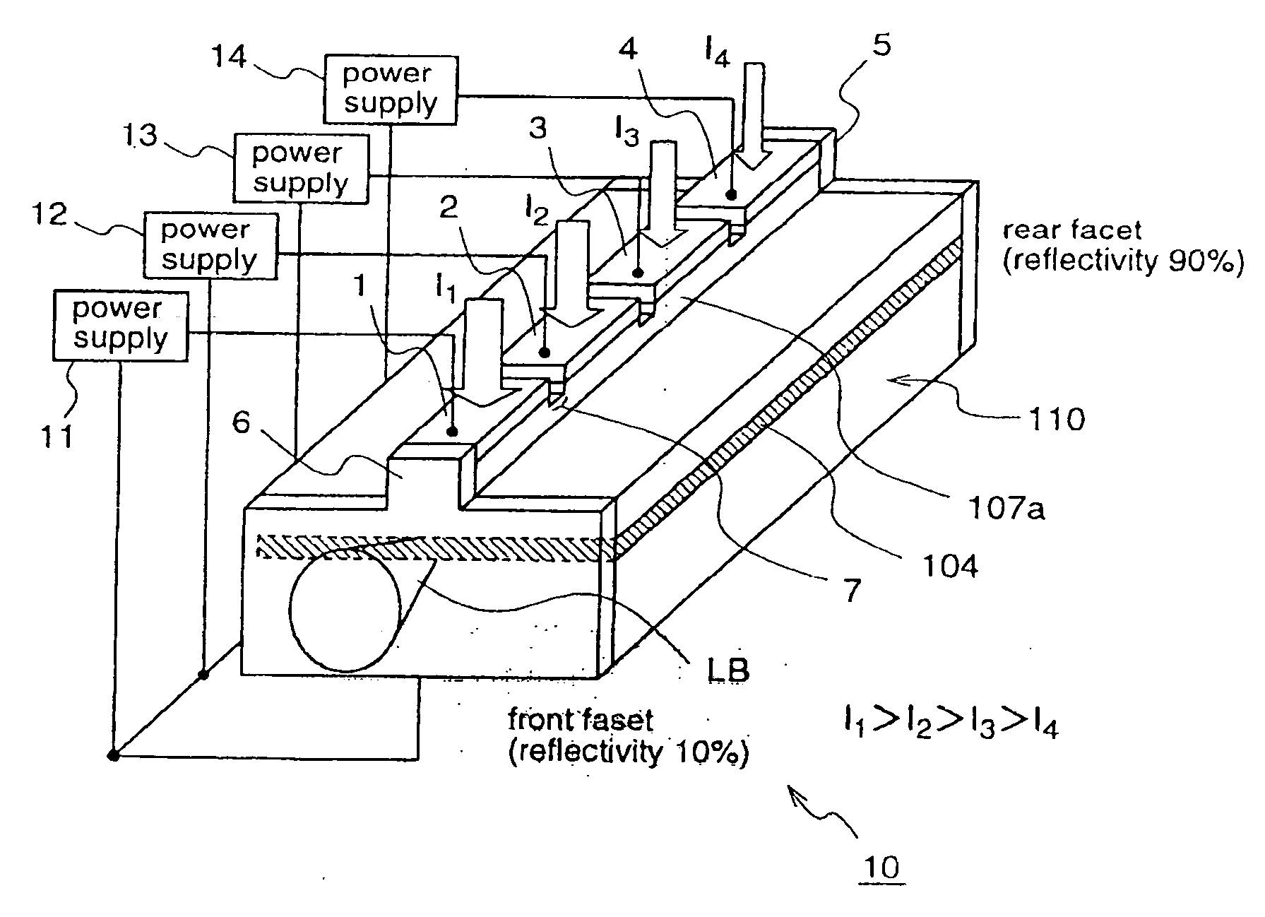
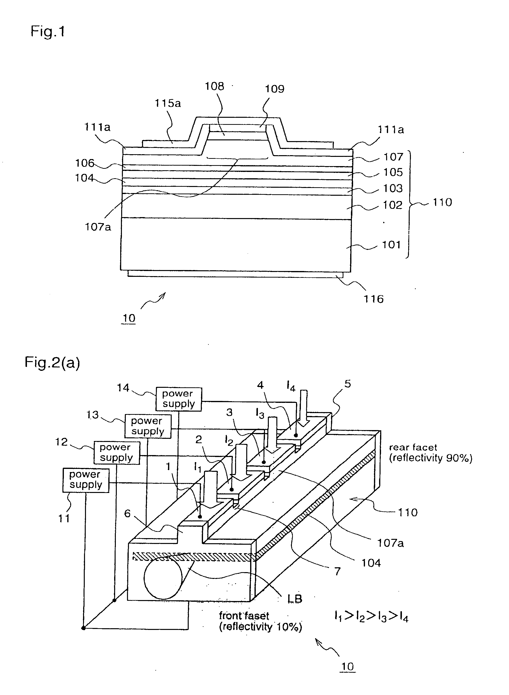
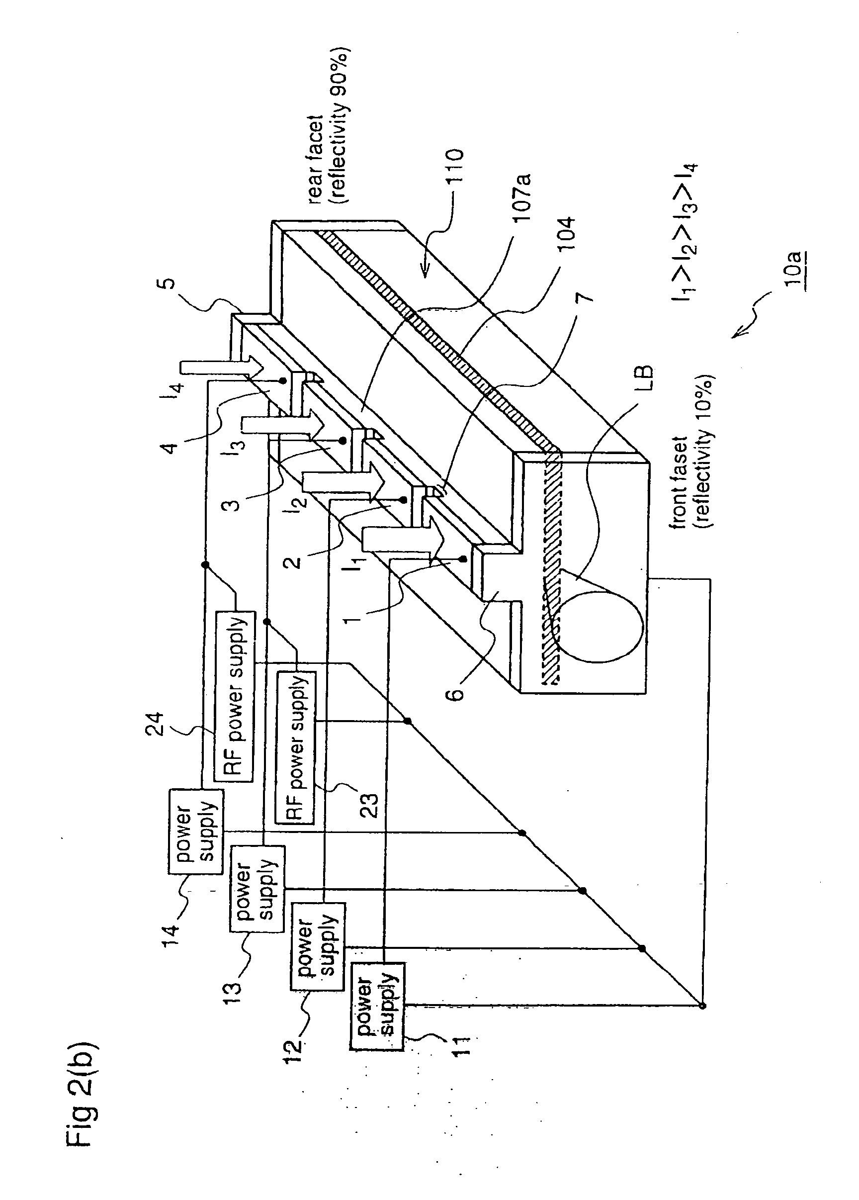
[0125] A semiconductor laser device according to a first embodiment of the present invention is a facet-emitting type semiconductor laser having a stripe structure for performing current constriction, in which a light reflectivity at a front facet from which light is emitted is different from a light reflectivity at a rear facet opposite to the front facet. An electrode disposed on the stripe structure is divided into plural electrode parts, and laser driving currents are applied to the respective electrode parts so that the density of current injected into an active layer becomes large at the front facet side and small at the rear facet side.

[0126] The semiconductor laser according to the first embodiment is applicable as a light source for an optical pickup or a laser display.

[0127] Hereinafter, the first embodiment will be described in detail.

[0128] Initially, a description will be given of a fundamental element structure of the semiconductor laser device according to the firs...

embodiment 2

[0180]FIG. 4 is a diagram for explaining a semiconductor laser device according to a second embodiment of the present invention.

[0181] The semiconductor laser device 20 according to the second embodiment is a high output semiconductor laser device of a wide-stripe structure, which is obtained by increasing the width of the stripe ridge 107a in the semiconductor laser device 10b of the first embodiment shown in FIG. 2(c), and it is utilized as a light source for a laser display.

[0182] That is, the semiconductor laser device 20 of this second embodiment has a semiconductor layer laminated body 110 which is obtained by successively depositing, on an n type GaN substrate, an n type AlGaN cladding layer, an n type GaN lightguide layer, an active layer having a multiquantum well structure including InGaN, an undoped GaN cap layer, a p type GaN lightguide layer, and a p type AlGaN cladding layer, like the semiconductor laser device 10 according to the first embodiment.

[0183] In this sec...

embodiment 3

[0206]FIG. 5 is a diagram for explaining a semiconductor laser device according to a third embodiment of the present invention, illustrating a plan view of a stripe ridge of the semiconductor laser device.

[0207] The semiconductor laser device 30 according to the third embodiment is obtained by tapering the plane surface of the stripe ridge 107a of the semiconductor laser device 10 according to the first embodiment such that the width of the stripe ridge 107a is larger as closer to the light emission facet, and other constituents are identical to those of the semiconductor laser device of the first embodiment.

[0208] That is, the semiconductor laser device 30 of this third embodiment has a semiconductor layer laminated body 110 which is obtained by successively depositing, on an n type GaN substrate, an n type AlGaN cladding layer, an n type GaN lightguide layer, an active layer having a multiquantum well structure including InGaN, an undoped GaN cap layer, a p type GaN lightguide l...


PUM


Abstract

According to the present invention, in a semiconductor laser device (10) having different facet reflectivities, an electrode disposed on a stripe ridge (107a) is divided into four electrode parts (1), (2), (3), and (4), and a larger injection current is injected to an electrode part that is closer to a light emission facet side. According to this semiconductor laser device, a carrier density distribution in an active layer that is opposed to the stripe ridge can be matched to a light intensity distribution in the active layer, thereby preventing degradation in high output characteristic due to destabilization of transverse mode and reduction in gain which are caused by spatial hole burning.

Description

TECHNICAL FIELD [0001] The present invention relates to a semiconductor laser device that operates stably at high output power, and more particularly, a semiconductor laser device using a III-V group nitride-base semiconductor material, and a laser projector using the semiconductor laser device. BACKGROUND ART [0002] With developments in optical communication and optical storage devices, demand for semiconductor lasers to be used therefor is growing, and a blue-violet semiconductor laser comprising a III-V group nitride-base semiconductor material such as gallium nitride (AlxGayIn1-x-yN; 0≦x1, 0≦y≦1) is actively developed as a key device for realizing a super high density recording on an optical disc. Particularly, increase in output power of the blue-violet semiconductor laser enables high-speed writing in an optical disc, and further, it is a technique indispensable for exploration of a new technical field such as application as a light source to a laser display which can represen...

Claims


Application Information

Patent Timeline
Patent Type & Authority Applications(United States)
IPC IPC(8): H01S3/00H01S5/00H01S3/097H01S5/042H01S5/062H01S5/0625H01S5/10H01S5/22
CPCH01S5/0287H01S5/0425H01S5/22H01S5/0625H01S5/1064H01S5/0624H01S5/04256
Inventor MIZUUCHI, KIMINORIYAMAMOTO, KAZUHISAKASAZUMI, KEN'ICHIKIDOGUCHI, ISAO
Owner PANASONIC CORP
Why Eureka
Try Eureka