Active matrix type semicondcutor display device

a display device and active matrix technology, applied in semiconductor devices, instruments, electrical appliances, etc., can solve problems such as display distortion, frame inversion system problems, and display quality degradation, and achieve the effects of reducing consumption of electric power, reducing voltage necessary, and improving reliability of elements

Inactive Publication Date: 2007-07-19
SEMICON ENERGY LAB CO LTD
View PDF34 Cites 19 Cited by
  • Summary
  • Abstract
  • Description
  • Claims
  • Application Information

AI Technical Summary

Benefits of technology

[0014] In an active matrix type semiconductor display device of the present invention, a counter electrode is divided into two, different electric potentials are applied to the two counter electrodes, respectively, and inversion driving is carried out each other. Since a voltage of an image signal can be made low by doing so, it is possible to lower a voltage necessary for operation of a driver circuit. As a result, it is possible to realize improvement of reliability of an element such as a TFT constituting the driver circuit and an active matrix circuit, and reduction of consumed electric power. Moreover, since it is possible to lower a voltage of a timing pulse supplied by the driver circuit, a booster circuit can be omitted, and reduction of an area of the driver circuit can be realized.
[0015] Accordingly, in the active matrix type semiconductor display device of the present invention, an addressing mode such as gate line (row) inversion driving, source line (column) inversion driving, or dot (point) inversion driving can be effectively adopted, and deterioration of a display screen can be prevented.

Problems solved by technology

The “burning” of the screen means a disturbance of display which occurs due to this hysteresis.
In recent years, while an active matrix type liquid crystal display device having high resolution / high fineness has been required, a problem of the frame inversion system becomes clear.
However, in the case where a liquid crystal is driven by the frame inversion system, when the time division driving system is used, a so-called crosstalk phenomenon may occur, which deteriorates the quality of a display screen through parasitic capacitance which can not be avoided in design.
As a result, such a state is caused that reliability of components such as TFTs making a driver circuit and an active matrix circuit is deteriorated, and consumed electric power of the driver circuit is increased.
Besides, in the case where the high potential side power source of higher voltage is used for a part of the driver circuit, it becomes necessary to provide a booster circuit for conversion into a signal of higher voltage required for screen display, and as a result, there occurs a problem that an area of the driver circuit becomes large.

Method used


Image

  • Active matrix type semicondcutor display device
  • Active matrix type semicondcutor display device
  • Active matrix type semicondcutor display device

Examples


embodiment 1

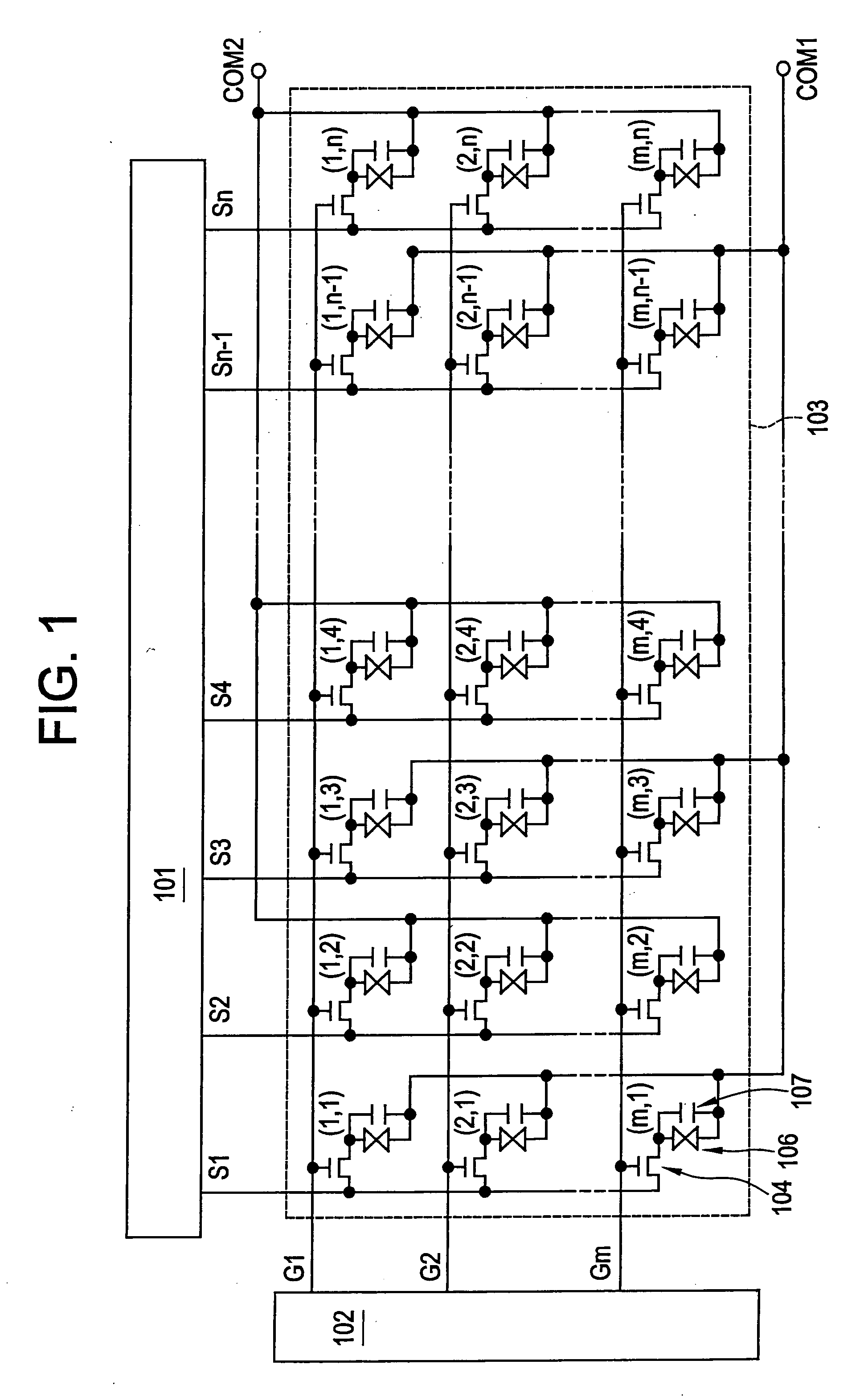
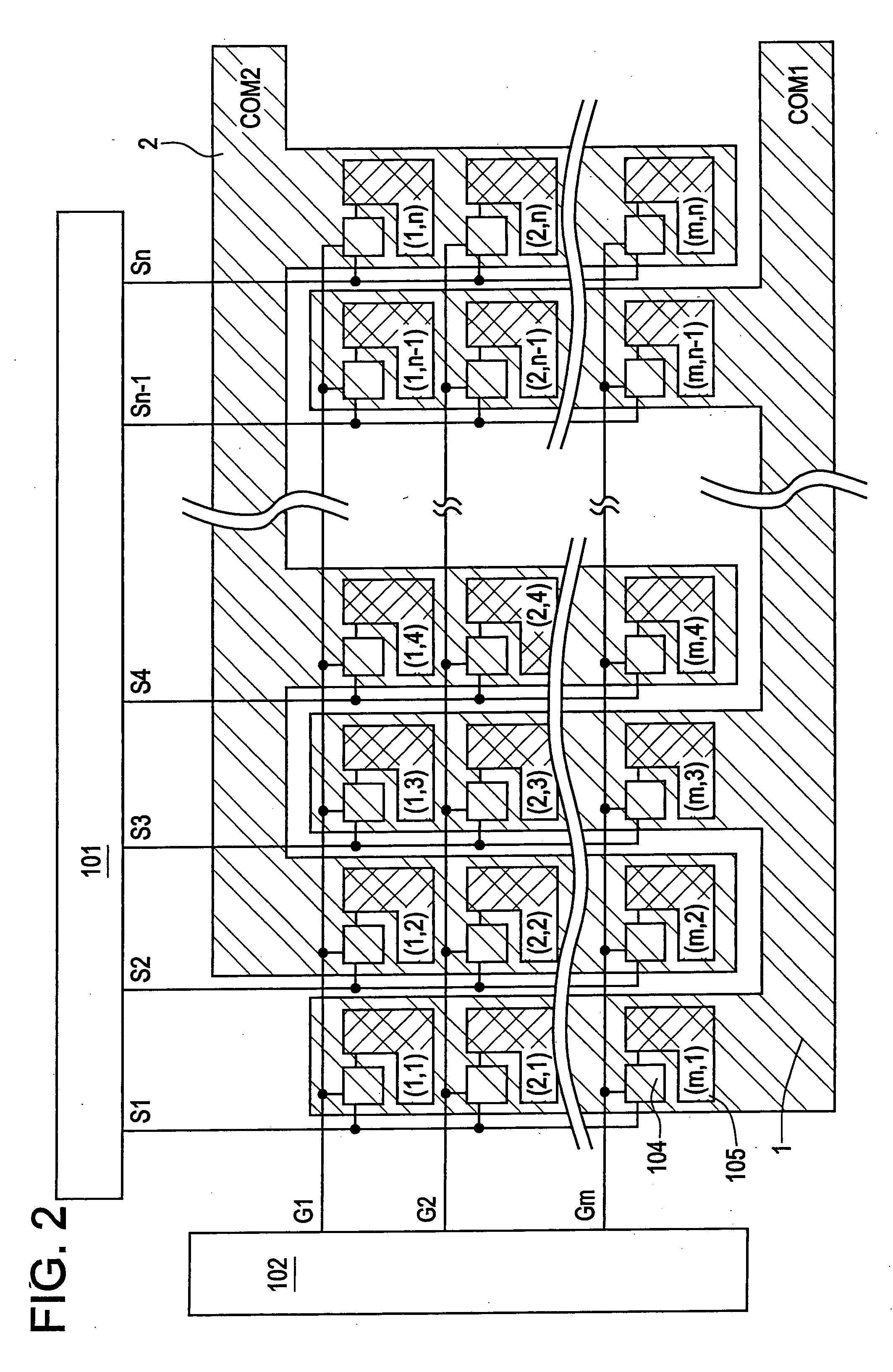
[0053] In this embodiment, an active matrix type display device of the present invention will be described by use of an active matrix type liquid crystal display device in which a liquid crystal is used as a display medium.

[0054] Reference will be made to FIG. 1. FIG. 1 is a schematic structural view showing an active matrix type liquid crystal display device of this embodiment. Reference numeral 101 designates a source signal line driver circuit; 102, a gate signal line driver circuit; and 103, an active matrix circuit. The active matrix circuit 103 is a portion where display of an image is made, and is constituted by a plurality of pixels. The active matrix type liquid crystal display device of this embodiment includes (m×n) pixels. Both n and m are natural numbers, and in this embodiment, n is an even number (m may be an even number or an odd number). For convenience of explanation, reference characters of (1, 1) to (m, n) are given to the respective pixels.

[0055] Each of the p...

embodiment 2

[0087] In this embodiment, a description will be made on an active matrix type liquid crystal display device which is different from the active matrix type liquid crystal display device of the embodiment 1 in the shape of a counter electrode and a driving method.

[0088] Reference will be made to FIG. 7. FIG. 7 is a schematic structural view of an active matrix type liquid crystal display device of this embodiment. Reference numeral 701 designates a source signal line driver circuit; 702, a gate signal line driver circuit; and 703, an active matrix circuit. The active matrix type liquid crystal display device of this embodiment includes (m×4n) (vertical×horizontal) pixels. Both n and m are natural numbers. For convenience of explanation, reference characters (1, 1) to (m, 4n) are given to the respective pixels. Since the structure of the active matrix circuit is the same as that of the embodiment 1, it is preferable to see the embodiment 1.

[0089] A pixel electrode (not shown) is con...

embodiment 3

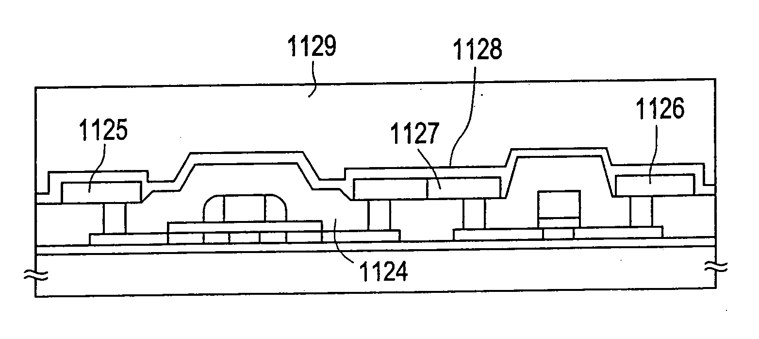
[0105] In this embodiment, a description will be made on an example of a fabricating method of the active matrix type liquid crystal display device described in the embodiment 1 and the embodiment 2. In this embodiment, an example in which a plurality of TFTs are formed on a substrate having an insulating surface, and an active matrix circuit, a driver circuit, and a logic circuit, etc. are monolithically constructed, will be described with reference to FIGS. 11E to 13D. In this embodiment, a state where a CMOS circuit as a basic circuit of the driver circuit, and the logic circuit, or the like will be described. Although the description will be made on the CMOS circuit in which a P-channel TFT (PTFT) and an N-channel TFT (NTFT) are respectively provided with one gate electrode, a CMOS circuit of a TFT provided with a plurality of gate electrodes, such as a double gate type or triple gate type, can be fabricated in the same manner. A pixel TFT is also formed of an N-channel TFT.

[01...


PUM


Abstract

There is provided an active matrix type semiconductor display device which realizes low power consumption and high reliability. In the active matrix type semiconductor display device of the present invention, a counter electrode is divided into two, different potentials are applied to the two counter electrodes, respectively and inversion driving is carried out each other. Since a potential of an image signal can be made low by doing so, it is possible to lower a voltage necessary for operation of a driver circuit. As a result, it is possible to realize improvement of reliability of an element such as a TFT and reduction of consumed electric power. Moreover, since it is possible to lower a voltage of a timing pulse supplied by the driver circuit, a booster circuit can be omitted, and reduction of an area of the driver circuit can be realized.

Description

BACKGROUND OF THE INVENTION [0001] 1. Field of the Invention [0002] The present invention relates to an active matrix type semiconductor display device, and particularly to an active matrix type liquid crystal display device. [0003] 2. Description of the Related Art [0004] In recent years, as an FPD (Flat Panel Display), an active matrix type semiconductor display device enlivens the market. Above all, an active matrix type liquid crystal display device has been frequently used as a display device of a personal computer. Further, in addition to a use for a note-sized personal computer, the active matrix type liquid crystal display device with a large screen comes to be used for a desktop personal computer. [0005] For the active matrix type liquid crystal display device used for a personal computer, in addition to a request for a large screen, it is required that plural pieces of information can be displayed at the same time. Then, the active matrix type liquid crystal display device...

Claims


Application Information

Patent Timeline
Patent Type & Authority Applications(United States)
IPC IPC(8): H01L21/00G09G3/32G09G3/36
CPCG02F2001/134318G09G3/3225G09G3/3233G09G3/3614G09G3/3655H01L27/1277G09G2300/0842G09G2310/0254G09G2310/0262G09G2330/021H01L27/12G09G2300/0465G02F1/134318
Inventor TANAKA, YUKIONAGAO, SHOU
Owner SEMICON ENERGY LAB CO LTD
Why Eureka
Try Eureka