Fabrication process of a semiconductor device

a technology of semiconductor devices and fabrication processes, which is applied in the direction of semiconductor devices, electrical devices, transistors, etc., can solve the problems of reducing the gate length and other problems, and achieve the effects of reducing the depth, increasing the leakage current, and low sheet resistan

Inactive Publication Date: 2007-07-19
FUJITSU SEMICON LTD
View PDF1 Cites 22 Cited by
  • Summary
  • Abstract
  • Description
  • Claims
  • Application Information

AI Technical Summary

Benefits of technology

[0014] According to such an elevated silicide formation technology, the Ni atoms on the surface part of the metallic nickel film are consumed by the silicide formation reaction caused by the silane gas by supplying the silane gas to the surface of the metallic nickel film at the time of the reaction between the metallic nickel film and the silicon surface as noted before, and the amount of the Ni atoms causing reaction with the silicon surface is reduced. With this, it becomes possible to reduce the depth of the silicide layer formation region invading into the silicon substrate.
[0016] Further, the inventor of the present invention has discovered, in the investigation that constitutes a foundation of the present invention, that there is easily formed a native oxide film on the surface of the nickel silicide layer of the Ni2Si phase, and as a result, there is caused variation of sheet resistance in the nickel silicide film of the NiSi phase. It is believed that such a native oxide film is formed as a result of exposure of the Ni2Si phase nickel silicide film to the air at the time the residual nickel film is removed by the selective wet etching process after formation of the nickel silicide layer of the Ni2Si phase according to the salicide process.
[0033] According to the present invention, invasion of Ni atoms from the nickel silicide layer of the Ni2Si phase into the silicon surface can be successfully suppressed by carrying out the thermal annealing process for converting the nickel silicide layer of the Ni2Si phase to the nickel monosilicide layer of the NiSi phase in the state of exposing the nickel silicide layer of the Ni2Si phase to the silane gas ambient. With this, it becomes possible to form the desired nickel monosilicide layer on the surface of the silicon region with a reduced depth, and the problem of the junction formed in the silicon region being destroyed by the diffusion of the Ni atoms and associated problem of variation and increase of the leakage current can be successfully eliminated. With such a construction, conversion to nickel monosilicide phase takes place also from the surface of the nickel silicide layer of the Ni2Si phase as a result of exposure to the silane gas, and as a result, it becomes possible to obtain the nickel monosilicide layer to have an extremely uniform and low sheet resistance.
[0034] Further, as a result of the reducing processing applied to the surface of the nickel silicide layer of the Ni2Si composition after removal of the metallic nickel film by the selective wet etching process but before conversion to the nickel monosilicide phase as a result of the thermal annealing processing applied to the nickel silicide layer of the Ni2Si composition, it becomes possible to reduce the sheet resistance of the obtained nickel monosilicide layer further.

Problems solved by technology

Today, there is already realized a semiconductor device having a gate length of 100 nm or less, while with such ultra-miniaturized semiconductor devices, there arise various problems in relation to decrease of the gate length.

Method used


Image

  • Fabrication process of a semiconductor device
  • Fabrication process of a semiconductor device
  • Fabrication process of a semiconductor device

Examples


first embodiment

[0047]FIGS. 1A-1L are diagrams showing the fabrication process of a semiconductor device 10 according to a first embodiment of the present invention, while FIG. 2 shows the flowchart corresponding to the steps of FIGS. 1H-1L.

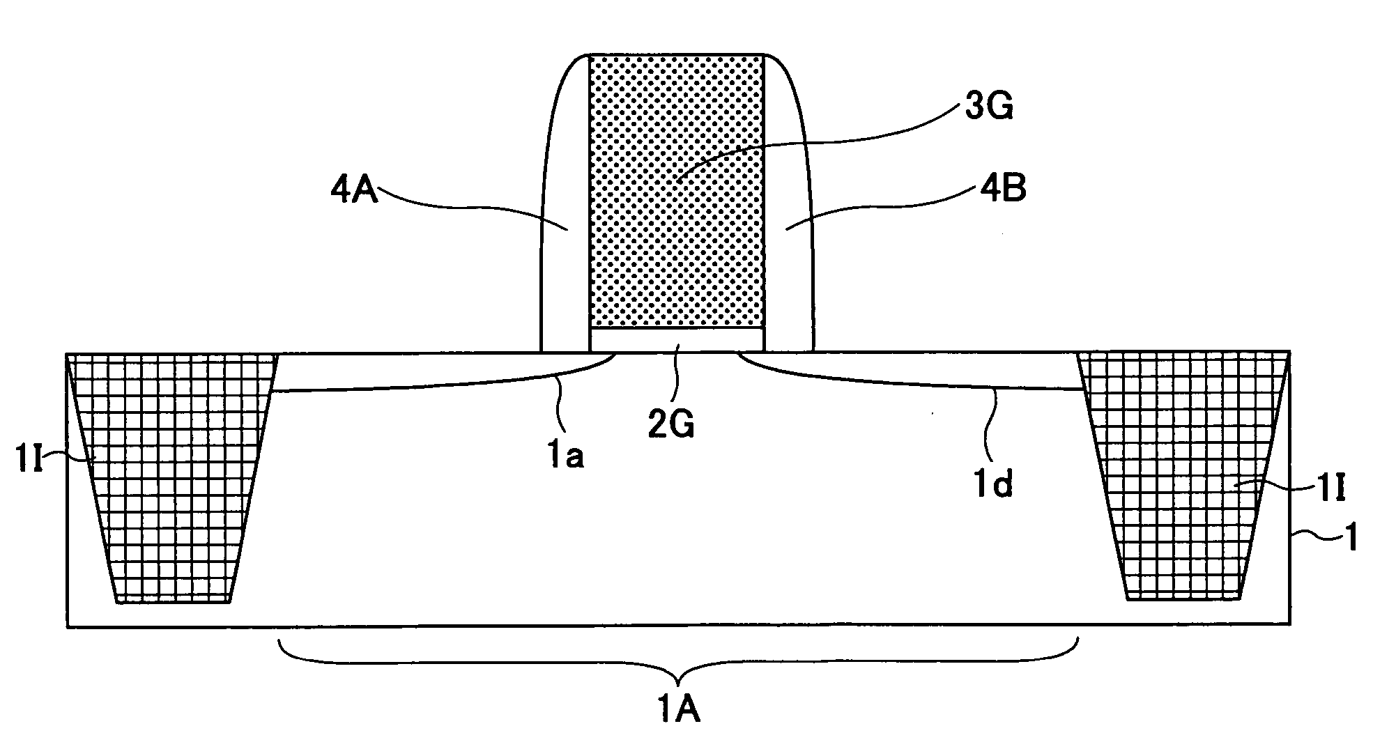
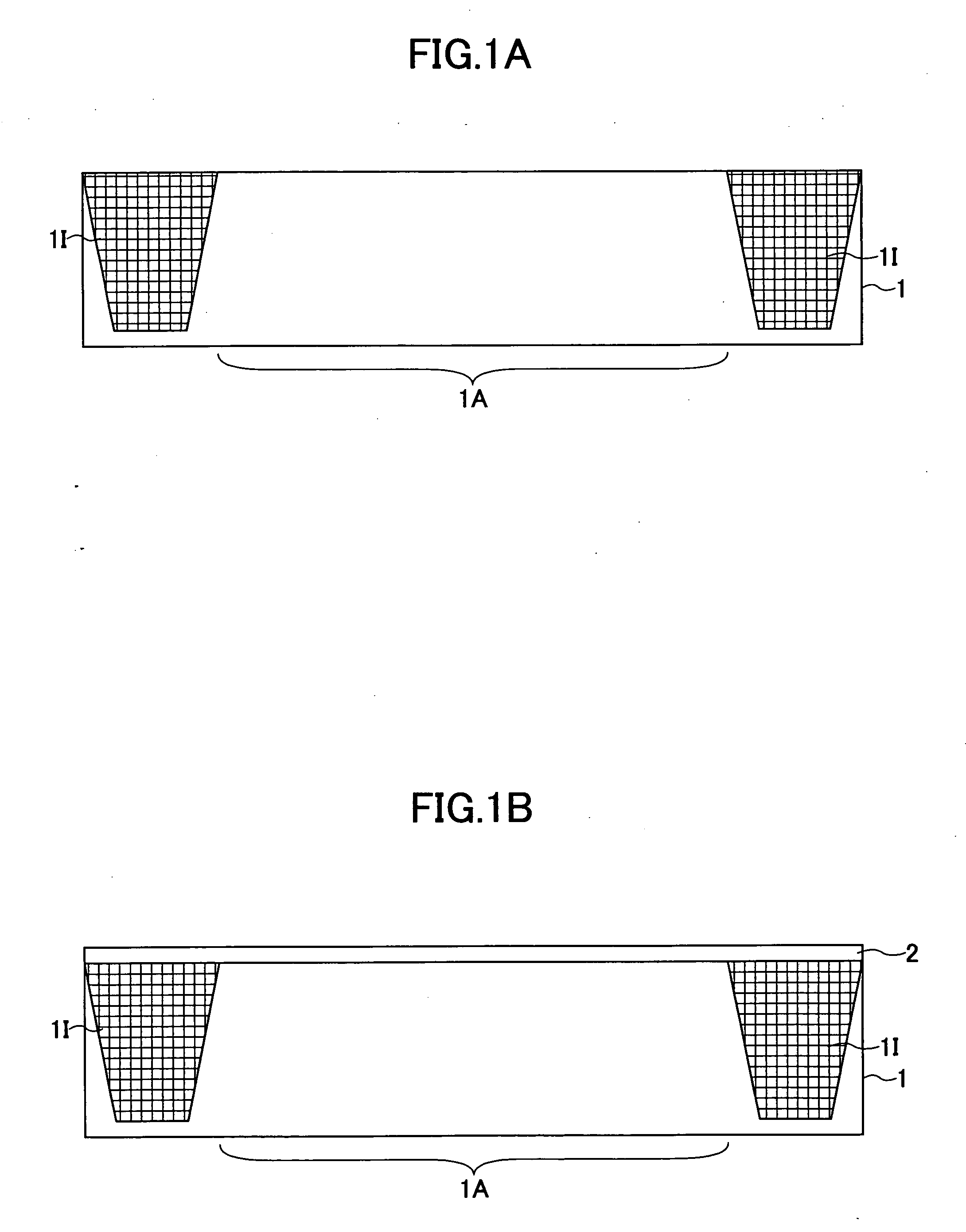
[0048] Referring to FIG. 1A, the semiconductor device 10 is an n-channel MOS transistor formed on a silicon substrate 1, wherein the silicon substrate is formed with a device region 1A by a device isolation region 1I of STI (shallow trench isolation) structure. The device region 1A may be formed with a p-type well (not shown), for example.

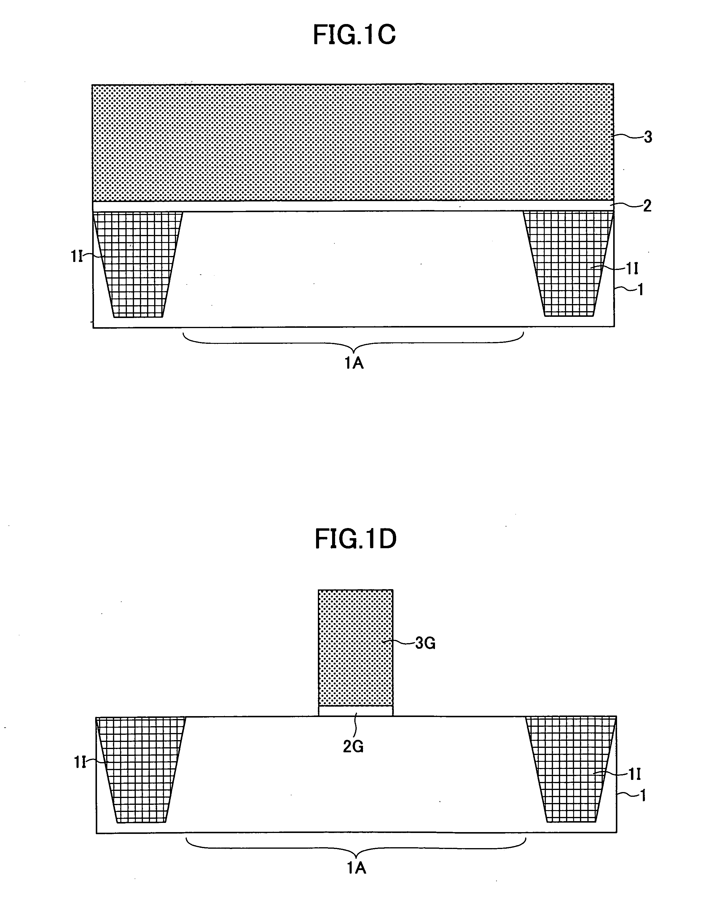
[0049] Next, in the step of FIG. 1B, an SiON film 2 is formed on the silicon substrate 1 with a thickness of 1-2 nm, and a polysilicon film 3 is formed on the SiON film 2 in the step of FIG. 1C.

[0050] Next, in the step of FIG. 1D, the polysilicon film and the SiON film 2 underneath thereof are subjected to a patterning process, and as a result, there are formed a polysilicon gate electrode 3G and an SiON gate insulation film...

second embodiment

[0075]FIGS. 8A-8E are diagrams showing the fabrication process of a semiconductor device according to a second embodiment of the present invention, wherein those parts corresponding to the parts described previously are designated by the same reference numerals and the description thereof will be omitted.

[0076] Referring to FIG. 8A, FIG. 8A represents the process step that follows the step of FIG. 1G and, after cleaning silicon surface by DHF or dry chemical cleaning, the metallic nickel film 5 is formed on the structure of FIG. 1G with the thickness of about 10 nm by a sputtering process, for example.

[0077] With the present embodiment, no protective film 5N is formed on the surface of the metallic nickel film 5, and the native oxide film of Ni formed on the surface of the metallic nickel film 5 is reduced to metallic Ni by annealing the structure of FIG. 8A in the hydrogen gas ambient in the subsequent process of FIG. 8B.

[0078] Next, in the step of FIG. 8C, the structure of the ...

third embodiment

[0083] Next, the fabrication process of a CMOS device according to a third embodiment of the present invention will be described with reference to FIGS. 9A-9F.

[0084] Referring to FIG. 9A, there are defined a device region 11A and a device region 11B respectively of an n-channel MOS transistor and a p-channel MOS transistor on a silicon substrate 11 by a device isolation structure 11I of STI type, wherein the device region 11A is doped to p-type and forms a p-type well. Further, the device region 11B is doped to n-type and forms an n-type well.

[0085] Further, in the device region 11A, ion implantation is conducted in the vicinity of the surface of the silicon substrate 11, although not illustrated, by a p-type impurity element for the purpose of threshold adjustment of the n-channel MOS transistor. Likewise, ion implantation is conducted in the vicinity of the surface of the silicon substrate 11 in the device region 11B, although not illustrated, by an n-type impurity element for t...


PUM

PropertyMeasurementUnit
temperatureaaaaaaaaaa
gate lengthaaaaaaaaaa

Abstract

A method of fabricating a semiconductor device comprises the step of forming a nickel monosilicide layer selectively over a silicon region defined by an insulation film by a self-aligned process. The self-aligned process comprises the steps of forming a metallic nickel film on a silicon substrate on which the insulation film and the silicon region are formed, such that the metallic nickel film covers the insulation film and the silicon region, forming a first nickel silicide layer primarily of a Ni2Si phase on a surface of the silicon region of the metallic nickel film by applying an annealing process to the silicon substrate, removing the metallic nickel film, after the step of forming the first nickel silicide layer, by a selective wet etching process, and converting the first nickel silicide layer to a second nickel silicide layer primarily of a NiSi phase by a thermal annealing process conducted in a silane gas.

Description

CROSS-REFERENCE TO RELATED APPLICATION [0001] The present application is based on Japanese priority application No. 2006-008946 filed on Jan. 17, 2006, the entire contents of which are hereby incorporated by reference. BACKGROUND OF THE INVENTION [0002] The present invention generally relates to semiconductor devices and more particularly to the fabrication process of a semiconductor device that includes a low-resistance nickel silicide film, particularly a nickel monosiliside film of a NiSi phase on an impurity diffusion region or gate electrode formed on a semiconductor substrate. [0003] In the art of MOS semiconductor integrated circuit devices, steady progress is being made with regard to improvement of integration density and miniaturization of device size for the purpose of achieving higher operational speed, further diversity of functions, larger memory capacity, further decrease of electric power consumption, or the like. Today, there is already realized a semiconductor devi...

Claims


Application Information

Patent Timeline
Patent Type & Authority Applications(United States)
IPC IPC(8): H01L21/4763
CPCH01L21/28518H01L21/324H01L21/823807H01L21/823814H01L21/823842H01L29/7848H01L29/665H01L29/6653H01L29/6659H01L29/66636H01L29/7833H01L29/518
Inventor UCHINO, YASUNORIKAWAMURA, KAZUOTAMURA, NAOYOSHI
Owner FUJITSU SEMICON LTD
Why Eureka
Try Eureka