Solar cell of high efficiency and process for preparation of the same

a solar cell and high efficiency technology, applied in the field of high-efficiency solar cells, can solve the problems of increased production costs, difficult to obtain the desired degree of anti-reflection efficiency, and need of expensive equipment such as laser equipment, so as to reduce the reflectivity of absorbed light, improve photoelectric conversion efficiency, and prevent the effect of carrier recombination

Inactive Publication Date: 2007-08-02
LG ELECTRONICS INC
View PDF8 Cites 48 Cited by
  • Summary
  • Abstract
  • Description
  • Claims
  • Application Information

AI Technical Summary

Benefits of technology

[0009] That is, the present invention has been made in view of the above problems, and it is an object of the present invention to provide a solar cell having a structure which is capable of improving a photoelectric conversion efficiency by further minimizing a reflectivity of absorbed light by a dual reflective film structure composed of a silicon oxynitride passivation layer and a silicon nitride anti-reflective layer, simultaneously with effective prevention of carrier recombination occurring at a semiconductor surface by the passivation layer.
[0010] It is another object of the present invention to provide a solar cell which is capable of achieving low-cost mass production capability by continuous formation of the dual reflective film structure via an in-situ process.

Problems solved by technology

However, since this technique employs the amorphous silicon thin film, it is difficult to obtain a desired degree of anti-reflection efficiency.
In addition, according to this Korean Patent, a baking process must be carried out at a low temperature of less than 450° C., and therefore a screen printing method cannot be used in formation of electrodes, thus resulting in a need of expensive equipment such as laser equipment.
That is, this method suffers from various problems such as complicated manufacturing processes and significantly increased production costs, thus making it difficult to enter practical application thereof.

Method used


Image

  • Solar cell of high efficiency and process for preparation of the same
  • Solar cell of high efficiency and process for preparation of the same

Examples


example 1

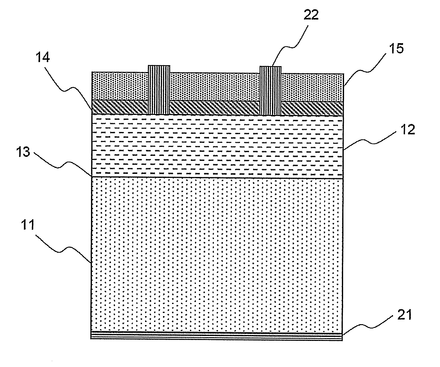
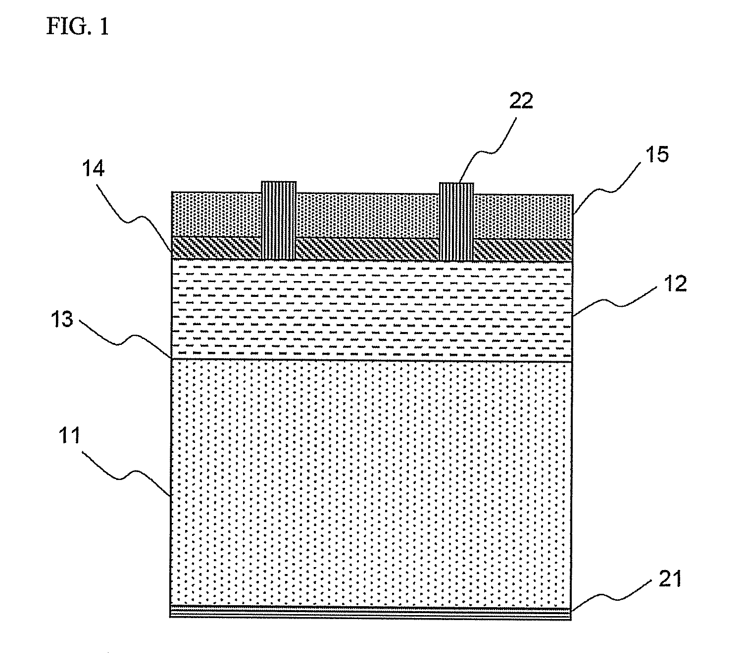
[0036] A phosphorus-doped n-type emitter layer was formed on a boron-doped p-type silicon substrate to result in a p-n junction. Silicon oxynitride (SiOxNy) as a passivation layer was deposited to a thickness of 30 nm on the n-type emitter layer, by a PECVD method. Then, silicon nitride (SiNx) having a refractive index of 1.9 as an anti-reflective layer was deposited on the silicon oxynitride passivation layer, by a PECVD method. Next, an Al-containing paste is screen-printed on the p-type silicon substrate and an Ag-containing paste is screen-printed on the silicon nitride layer, thereby forming a pattern. The resulting structure was baked at a temperature of around 800° C. for about 30 sec to simultaneously form a rear electrode connected to the p-type silicon substrate and a front electrode connected to the n-type emitter layer, thereby fabricating a solar cell.

experimental example 1

[0039] In order to measure an efficiency of solar cells fabricated in Example 1 and Comparative Examples 1 and 2, open-circuit voltage (Voc) and short-circuit current (Jsc) were respectively measured. Then, based on the thus-measured Voc and Jsc values, a fill factor (FF) and the solar cell efficiency were measured. The results thus obtained are set forth in Table 1. Herein, the fill factor (FF) is defined as (Vmp×Jmp) / (Voc×Jsc), where Jmp and Vmp represent the current density and voltage at the maximum power point. The solar cell efficiency is given as Pmax / Pin, where Pmax represents the maximum power generated by the cell and the power input, Pin, into the system is defined to be the incident light intensity, i.e., the light energy supplied to the system per unit time.

TABLE 1Composition ofEfficiencyExample No.reflective filmJsc (mA)Voc (V)FF (%)(%)Ex. 1SiOxNy / SiNx32.70.62079.016.01Comp. Ex. 1SiO2 / SiNx32.70.61678.815.87Comp. Ex. 2SiNx32.40.61878.515.71

[0040] As can be seen from t...


PUM


Abstract

Disclosed herein is a high-efficiency solar cell. More specifically, provided is a solar cell comprising a first conductivity type semiconductor substrate, a second conductivity type semiconductor layer formed on the first conductivity type semiconductor substrate and having a conductivity type opposite to that of the substrate, a p-n junction at an interface therebetween, a rear electrode in contact with at least a portion of the first conductivity type semiconductor substrate, a front electrode in contact with at least a portion of the second conductivity type semiconductor layer, and a silicon oxynitride passivation layer and a silicon nitride anti-reflective layer sequentially formed on a rear surface of the first conductivity type semiconductor substrate and/or a front surface of the second conductivity type semiconductor layer; and a process for preparing the same. Therefore, the solar cell according to the present invention can improve a photoelectric conversion efficiency by minimizing a reflectivity of absorbed light via provision of a dual reflective film structure composed of the passivation layer and anti-reflective layer, simultaneously with effective prevention of carrier recombination occurring at a semiconductor surface by the passivation layer. Further, the present invention enables a significant reduction of production costs by mass production capability via in situ continuous formation of the dual reflective film structure.

Description

FIELD OF THE INVENTION [0001] The present invention relates to a high-efficiency solar cell. More specifically, the present invention relates to a solar cell which is capable of improving a photoelectric conversion efficiency by minimizing a reflectivity of absorbed light by a dual reflective film structure composed of a passivation layer and an anti-reflective layer, in conjunction with effective prevention of carrier recombination occurring at a semiconductor surface by the passivation layer, via sequential formation of a silicon oxynitride passivation layer and a silicon nitride anti-reflective layer on a second conductivity type semiconductor layer forming a p-n junction with a first conductivity type semiconductor substrate and having a conductivity type opposite to that of the first conductivity type semiconductor substrate. Further, the present invention provides a process for preparing a solar cell, which is capable of reducing production costs by mass production capability ...

Claims


Application Information

Patent Timeline
Patent Type & Authority Applications(United States)
IPC IPC(8): H01L31/00
CPCY02E10/52H01L31/02168Y02E10/50H01L31/0216H01L31/04H01L31/06H01L31/18
Inventor PARK, HYUN JUNG
Owner LG ELECTRONICS INC
Why Eureka
Try Eureka