Etch resistant heater and assembly thereof

a heater and etch-resistant technology, applied in the direction of coatings, metallic material coating processes, chemical vapor deposition coatings, etc., can solve the problems of increasing the lifetime of the heater, not always practicable in some applications to establish physical contact between the surface, and inability to transfer heat from the heating element to the wafer, so as to improve the thermal uniformity of the wafer, improve the temperature uniformity, and save the effect of heat generation

Inactive Publication Date: 2007-08-09
GENERAL ELECTRIC CO
View PDF23 Cites 11 Cited by
  • Summary
  • Abstract
  • Description
  • Claims
  • Application Information

AI Technical Summary

Benefits of technology

[0012]In one embodiment, the overcoating layer has a planar thermal conductivity of at least 3 times the planer thermal conductivity of the first outer coating so that it also improves the temperature uniformity on the radiating surface of the heater, which then has a direct improvement on the thermal uniformity of the wafers. In a third embodiment, the overcoating layer comprises pyrolytic graphite.
[0013]In another aspect, the invention relates to a thermal module for use in high temperature semiconductor processes such as MOCVD. The thermal module contains the above-defined heater as the radiant heating element. In one embodiment, the module further includes a reflector stack comprising a high reflective material placed below the heater to better conserve the heat generated. Additional tubular reflector shields and covers may also be added to help even better conservation of the heater power.

Problems solved by technology

After a deposition of a film of predetermined thickness on the silicon wafer, there is a spurious deposition on other exposed surfaces inside the reactor, including the reactor walls, reactor windows, gas injector surfaces, exhaust system surfaces, and the substrate holder surfaces exposed to the deposition process.
This spurious deposition could present problems in subsequent depositions, and is therefore periodically removed with a cleaning process, i.e. in some cases after every wafer and in other cases after a batch of wafers has been processed.
However, it is not always practical in some applications to establish physical contact between the surface to be heated and the heating element.
The heat transfer from the heating element to the wafers is not possible both by convection (due to vacuum conditions) and by conduction (due to non-contact).
This approach will increase the lifetime of the heater but reduces the overall throughput substantially.
Heating by high intensity lamps does not always give the desired temperature uniformity on the wafer surface.
Multi-zone lamps may be used to improve temperature uniformity, but they increase costs and maintenance requirements.
In addition, many lamps use a linear filament, which makes them ineffective at providing uniform heat to a round wafer.
Most resistive heaters in the prior art tend to have a large thermal mass, which makes them unsuitable for high temperature applications of >1500° C. on the graphite susceptor.
Unfortunately, the sintered AlN substrate holders of the prior art suffer from an important limitation, namely they can only be heated or cooled at a rate of <20° C. / min.
If ramped any faster, the ceramic will typically crack.
Furthermore, only moderate temperature differentials can be sustained across a substrate surface before the ceramic will crack.
However, for very high temperature applications, i.e., where the required heater temperatures are >1500° C., a silicon carbide coating will not work well since silicon carbide decomposes at such high temperatures.
On the other hand, heaters with a boron carbide outer coating layer is technically feasible but not commercially practical to manufacture.

Method used


Image

  • Etch resistant heater and assembly thereof
  • Etch resistant heater and assembly thereof
  • Etch resistant heater and assembly thereof

Examples


examples 1 and 2

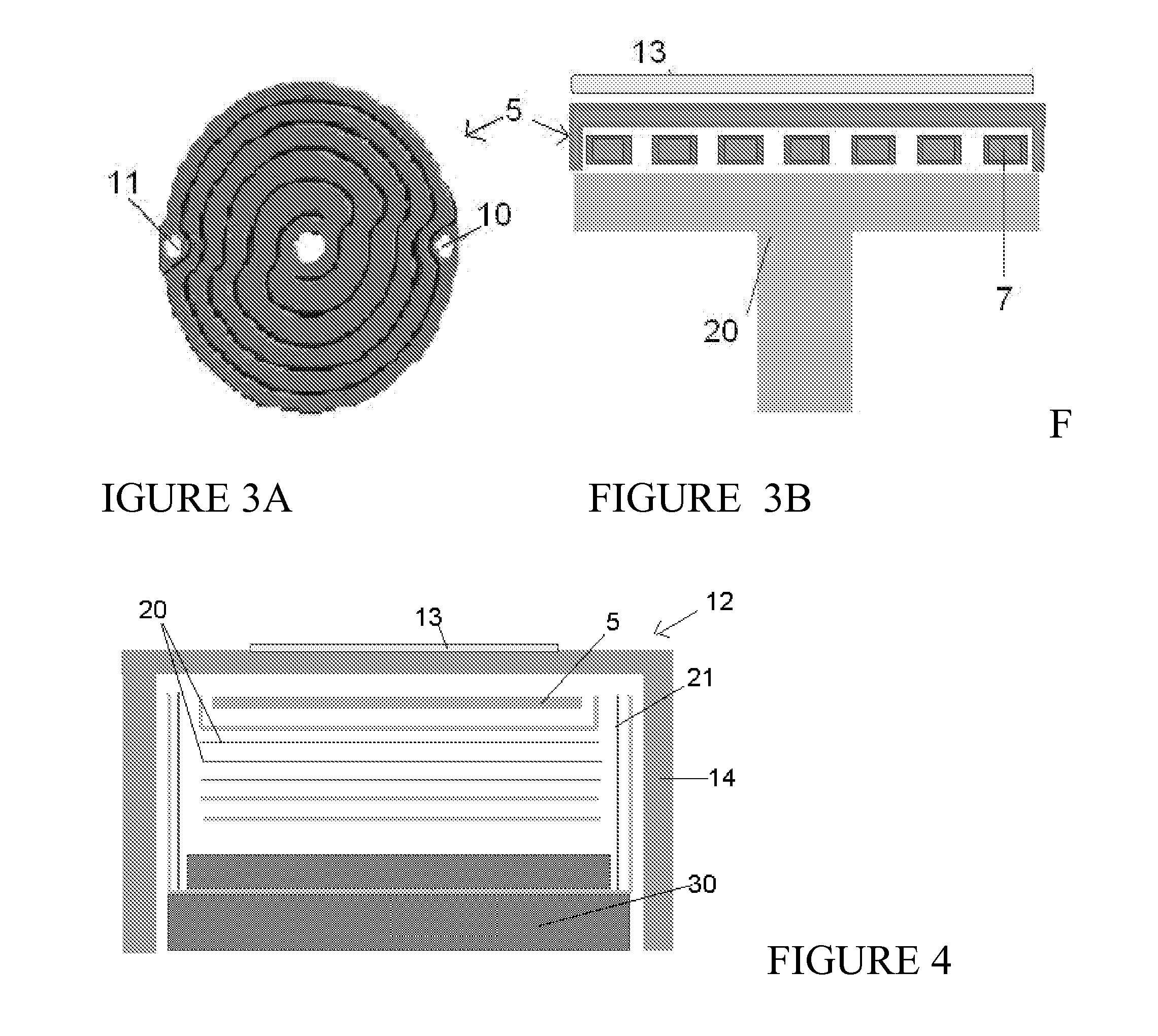
[0064]Computational fluid dynamics (CFD) calculations are carried out to model the thermal modules (heater assemblies). The first thermal module 12 employs a ceramic heater in the prior art as illustrated in FIG. 4. The same thermal module 12 employs one embodiment of the heater of the invention as illustrated in FIG. 5. The modules are to heat a single 2″ inch wafer to 1300° C. with a uniformity of around ±3° C. Uniformity requirement is extremely stringent in the case of Metal Organic Chemical Vapor Deposition (MOCVD) process. Hence, every Celsius degree variation in temperature uniformity affects the deposition process. Temperature uniformity on the wafer surface is defined as the difference between the maximum temperature and minimum temperature as measured by 9 thermocouples placed across the wafer surface.

[0065]As shown in the Figures, wafer 13 is placed on a susceptor 14 which is rotating and hence cannot be in direct contact with the heater 5. The base plate 30 comprises gra...

example 3

[0073]In this example, a radiant ceramic heater of the prior art is experimentally tested in an enclosed thermal module 90 as illustrated in FIGS. 9A-9B. In 9A, the ceramic heater 5 has a pBN core plate with a diameter of about 40 mm and a thickness of 2 mm, a thin patterned electrode of pyrolytic graphite, and an overcoating layer comprising pBN of a thickness of 0.15 mm. The enclosed thermal module 90 has an ambient pressure of 30 pa (close to vacuum condition). The heater 5 is surrounded by concentric cylinder tubes (90 mm in diameter) comprising pBN 93, Mo 94, and graphite 95, which function as radiation shields. In FIG. 9B, a stack of reflector plates 97 comprising pBN and Mo are placed below the heater to help conserve the heat by reflecting by towards the graphite susceptor 91, which is positioned 3-5 mm above the heater top surface. The susceptor having a diameter of 55 mm is heated only by thermal radiation.

[0074]A wafer is placed on the susceptor 91, which rotates and cann...

example 4

[0075]This is a duplicate of Example 3, except that a heater of the present invention is used. In this example, a 40 mm diameter ceramic heater with a pBN core plate with a diameter of about 40 mm and a thickness of 2 mm, a thin patterned electrode of pyrolytic graphite, and an overcoating layer comprising PBN of a thickness of 0.15 mm. Over this coating, the heater is further provided with a top overcoating layer of pyrolytic graphite of about 40 μm thick.

[0076]Table 2 presents data obtained from the operation of the thermal modules of Examples 3 and 4 in heating the susceptor when the heater is steadily maintained at 1700° C. Data is also illustrated in FIG. 10A-10B comparing the ramping tests of the two heaters.

TABLE 2ExampleHeater TypeSusceptor T ° C.Heater T° C.3PBN Heater110017004PG Overcoated PBN Heater13801700

[0077]As illustrated in Table 2, when both heaters are set to the same T of 1700° C., the susceptor T for the heater of the invention (Example 4—PG overcoated PBN heate...


PUM

PropertyMeasurementUnit
temperatureaaaaaaaaaa
thicknessaaaaaaaaaa
thicknessaaaaaaaaaa

Abstract

An etch resistant heater for use in a wafer processing assembly with an excellent ramp rate of at least 20° C. per minute. The heater is coated with a protective overcoating layer allowing the heater to have a radiation efficiency above 70% at elevated heater temperatures of >1500° C., and an etch rate in NF3 at 600° C. of less than 100 A / min.

Description

CROSS-REFERENCE TO RELATED APPLICATIONS[0001]This application claims the benefits of U.S. Patent Application Ser. No. 60 / 771,745, with a filing date of Feb. 9, 2006; and U.S. Patent Application Ser. No. 60 / 744741 with a filing date of Apr. 12, 2006, which patent applications are fully incorporated herein by reference.FIELD OF THE INVENTION[0002]The invention relates generally to a heater and a heater assembly, for use in the fabrication of electronic devices.BACKGROUND OF THE INVENTION[0003]The process for fabrication of electronic devices, including integrated circuits (ICs), micro-electromechanical systems (MEMs), optoelectronic devices, flat panel display devices, comprises a few major process steps including the controlled deposition or growth of materials and the controlled and often selective removal or modification of previously deposited / grown materials. Chemical Vapor Deposition (CVD) is a common deposition process, which includes Low Pressure Chemical Vapor Deposition (LPC...

Claims


Application Information

Patent Timeline
Patent Type & Authority Applications(United States)
IPC IPC(8): C23C16/00
CPCC23C16/4581H01L21/67103C23C16/46H01L21/6831H01L21/68757C23C16/4586C23C16/4405
Inventor OTAKA, AKINOBUHIGUCHI, TAKESHIPRASAD, SRIDHAR RAMAPRASADFAN, WEISCHAEPKENS, MARCLONGWORTH, DOUGLAS A.
Owner GENERAL ELECTRIC CO
Why Eureka
Try Eureka