Eureka AIR delivers breakthrough ideas for toughest innovation challenges, trusted by R&D personnel around the world.

CMOS image sensor

Active Publication Date: 2007-08-09
SEMICON MFG INT (SHANGHAI) CORP +1
View PDF11 Cites 8 Cited by
  • Summary
  • Abstract
  • Description
  • Claims
  • Application Information

AI Technical Summary

Problems solved by technology

However, CCD imagers also suffer from a number of disadvantages.
For example, they are susceptible to radiation damage, they exhibit destructive read out over time, they require good light shielding to avoid image smear and they have a high power dissipation for large arrays.
Additionally, while offering high performance, CCD arrays are difficult to integrate with CMOS processing in part due to a different processing technology and to their high capacitances, complicating the integration of on-chip drive and signal processing electronics with the CCD array.
While there have been some attempts to integrate on-chip signal processing with the CCD array, these attempts have not been entirely successful.
CCDs may also suffer from incomplete charge transfer from pixel to pixel during charge transfer which also results in image smear.

Method used


Image

  • CMOS image sensor
  • CMOS image sensor

Examples


Embodiment Construction

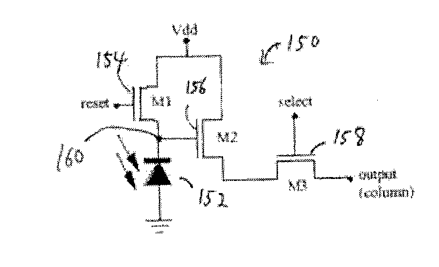
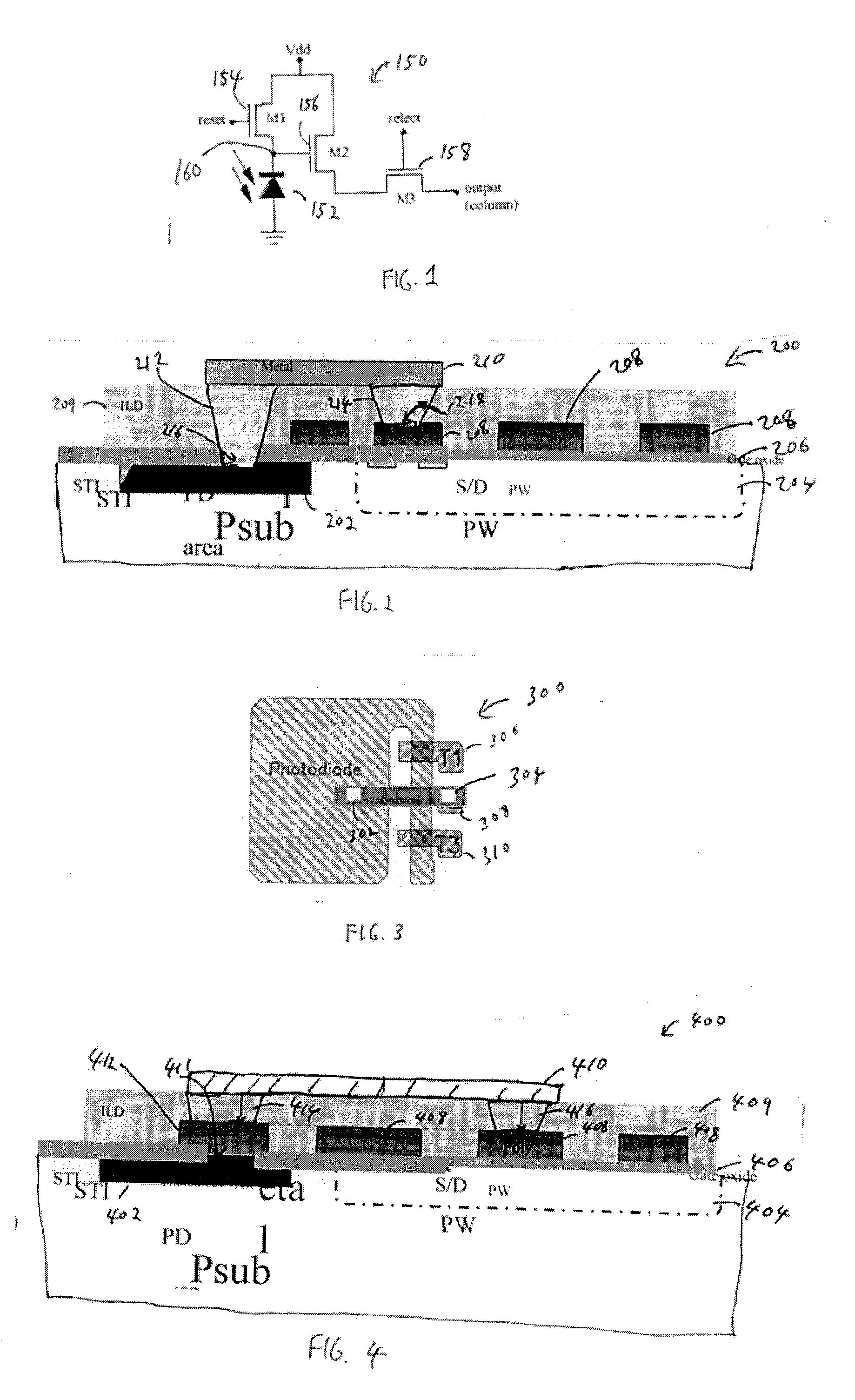
[0015] The present invention relates to CMOS image sensors with reduced junction leakage, e.g., dark current. FIG. 1 illustrates a circuit 150 of a pixel cell in a CMOS image sensor. The pixel cell is a three-transistor (3T) design. The circuit 150 includes a photodiode 152, a reset transistor 154, a source follower transistor 156, and a row select transistor 158. A node 160 couples the photodiode, reset transistor, and source follower transistor.

[0016]FIG. 2 illustrates a schematic cross-section of a 3T pixel cell 200. A photodiode 202 is provided on a silicon substrate. A source / drain region 204 is provided at a given distance from the photodiode. A gate oxide layer 206 is provided over the photodiode 202 and the source / drain region 204. A plurality of gates 208 are formed over the gate oxide. These gates are the gates for the reset transistor, source follower transistor, and row select transistor. An inter-layer dielectric (ILD) 209 is formed over the gates 208. A metal layer 21...


PUM


Abstract

A complementary metal oxide semiconductor (CMOS) image sensing device includes a semiconductor substrate; a photodiode defined on the substrate; a gate dielectric layer provided over the photodiode and the substrate; a polysilicon interconnect contacting a given area of the photodiode via an opening in the gate dielectric layer; a reset transistor coupled to the photodiode; a source follower transistor coupled to the photodiode; and a select transistor coupled to the source follower transistor. The given area of the photodiode defines a node that is coupled to the reset transistor and source follower transistor.

Description

CROSS REFERENCE TO RELATED APPLICATIONS [0001] This application claims priority to Chinese Application No. 200610024139.5, filed on Feb. 24, 2006, commonly assigned, and of which is hereby incorporated by reference for all purposes. BACKGROUND OF THE INVENTION [0002] The present invention relates to a CMOS image sensor having a contact structure including polysilicon. [0003] Two common types of semiconductor-based imagers are charge coupled devices (CCDs) and complementary metal oxide semiconductor (CMOS) devices. CCDs are often employed for image acquisition and enjoy a number of advantages which makes it the incumbent technology, particularly for small size imaging applications. CCDs are also capable of large formats with small pixel size and they employ low noise charge domain processing techniques. However, CCD imagers also suffer from a number of disadvantages. For example, they are susceptible to radiation damage, they exhibit destructive read out over time, they require good ...

Claims


Application Information

Patent Timeline
IPC IPC(8): H01L31/113
CPCH01L27/14609
Inventor HUO, JIE GUANGYANG, JIANPINGXIN, CHUN YAN
Owner SEMICON MFG INT (SHANGHAI) CORP
Why Eureka
Eureka Blog
Learn More