Dry etching method, fine structure formation method, mold and mold fabrication method

Inactive Publication Date: 2007-08-16
PANASONIC CORP
View PDF10 Cites 232 Cited by
  • Summary
  • Abstract
  • Description
  • Claims
  • Application Information

AI Technical Summary

Benefits of technology

[0069] In any of the dry etching method, the fine structure formation method, the mold fabrication method and the mold of this invention, when the substance including tungsten and carbon further includes nitrogen (N), the same effects as described above can be attained. In other words, when the invention is applied to a WCN alloy, a WNC alloy or the like, the same effects can be attained.
[0070] As described so far, the dry etching method of this invention is useful for highly precisely microprocessing a substance including tungsten

Problems solved by technology

In the conventional dry etching method using CF4 or SF6, however, not only the bottom of a pattern but also the side face of the pattern is etched so that the side face is formed in a bowing shape as described above, and hence, a vertical etching shape cannot be attained and high performance processi

Method used


Image

  • Dry etching method, fine structure formation method, mold and mold fabrication method
  • Dry etching method, fine structure formation method, mold and mold fabrication method
  • Dry etching method, fine structure formation method, mold and mold fabrication method

Examples


embodiment 1

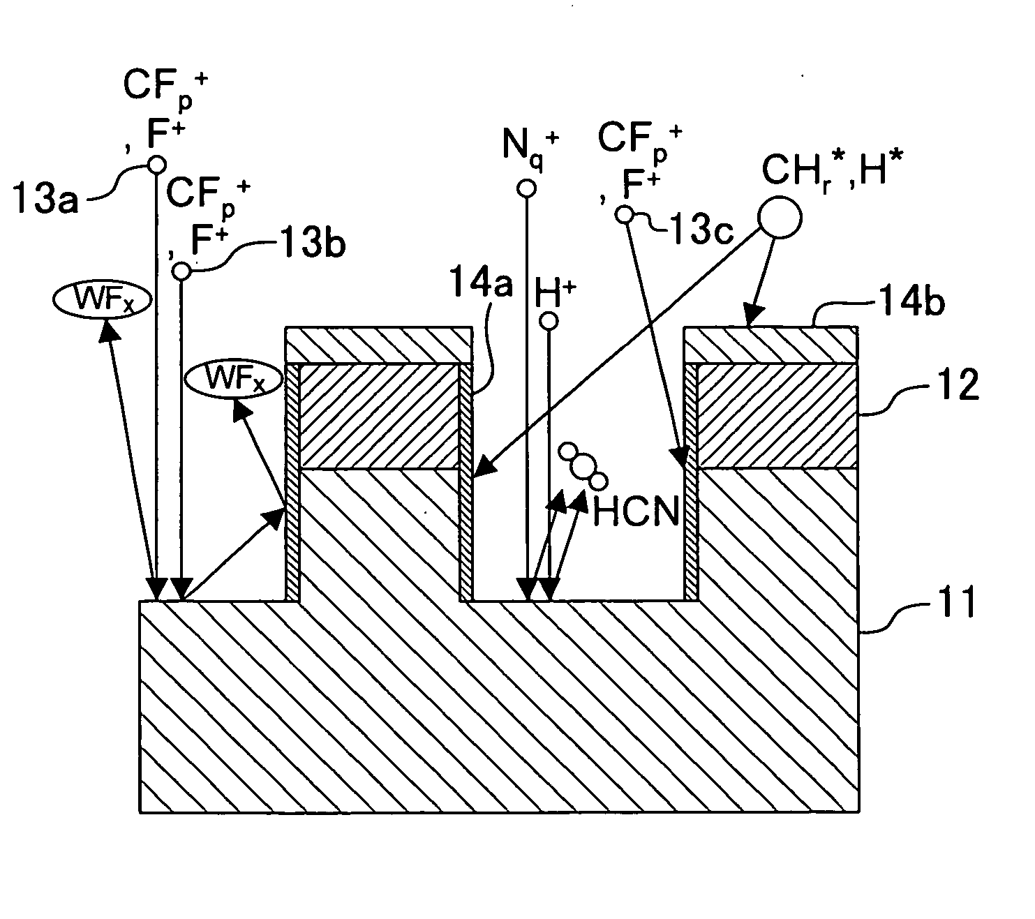
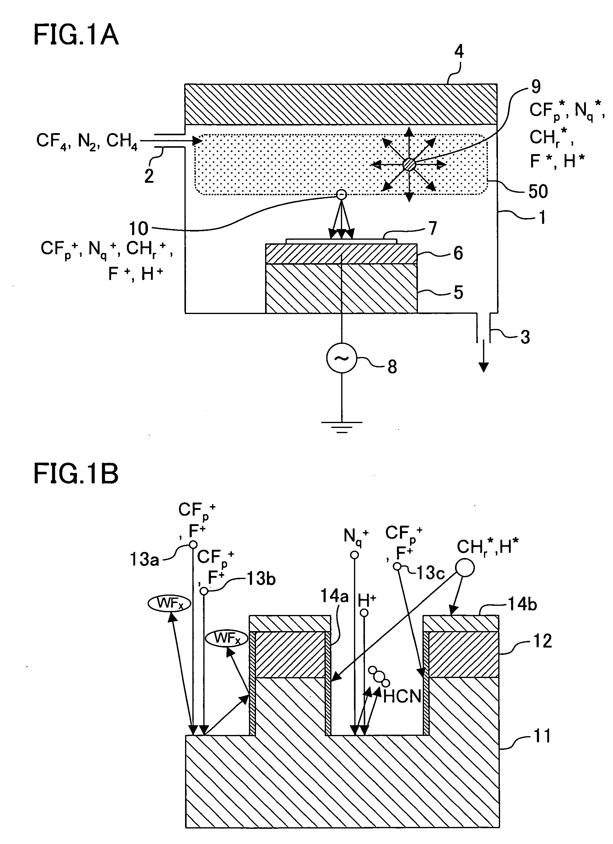
[0079] A dry etching method according to Embodiment 1 of the invention will now be described with reference to the accompanying drawings.

[0080]FIGS. 1A and 1B are explanatory diagrams of the dry etching method of Embodiment 1 of the invention. As shown in FIG. 1A, a reaction chamber 1 in which a reduced pressure can be kept is provided with a gas inlet 2 and a gas outlet 3. Also, a plasma generator 4 for changing a gas supplied through the gas inlet 2 into plasma is provided in an upper portion of the reaction chamber 1. Furthermore, an electrode 6 on which a target substance including tungsten and carbon, specifically, a WC alloy substrate or a substrate having a WC alloy in its surface portion (hereinafter both referred to as a WC substrate 7), is placed is provided on an insulator 5 in a lower portion of the reaction chamber 1. An RF (radio frequency) power source 8 for applying a bias voltage to the electrode 6 is provided outside the reaction chamber 1.

[0081] Next, the operat...

embodiment 2

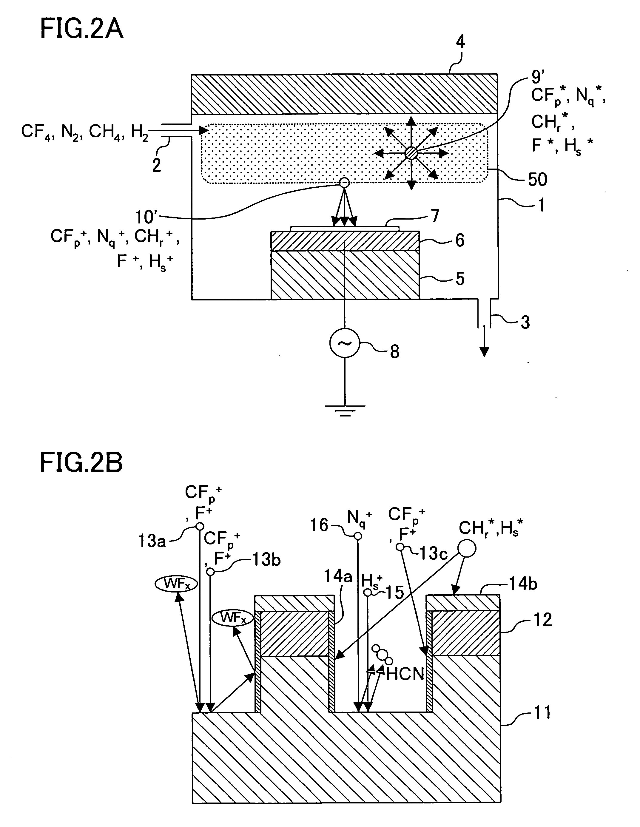
[0103] Now, a dry etching method according to Embodiment 2 of the invention will be described with reference to the accompanying drawings. A difference of the dry etching method of this embodiment from that of Embodiment 1 is that a substance including tungsten and carbon as principal compositions is dry etched by using plasma generated with a gas including a hydrogen atom (such as a hydrogen molecule or an ammonia molecule) further added to the mixed gas of the gas including a fluorine atom, the gas including a nitrogen atom and the gas including a hydrocarbon molecule.

[0104]FIGS. 2A and 2B are explanatory diagrams of the dry etching method of Embodiment 2 of the invention. In FIGS. 2A and 2B, like reference numerals are used to refer to like elements used in Embodiment 1 so as to omit the description. Also, in FIGS. 2A and 2B, a mixed gas of CF4, N2, CH4 and H2 is used as an etching gas.

[0105] As shown in FIG. 2A, a difference of this embodiment from Embodiment 1 is that radical...

embodiment 3

[0110] Now, a dry etching method according to Embodiment 3 of the invention will be described with reference to the accompanying drawings. A difference of the dry etching method of this embodiment from that of Embodiment 1 is that a substance including tungsten and carbon as principal components is dry etched by using plasma generated with at least one of a gas including a chlorine atom, a gas including a bromine atom and a gas including an iodine atom further added to the mixed gas of the gas including a fluorine atom, the gas including a nitrogen atom and the gas including a hydrocarbon molecule. In other words, an ion including a chlorine atom, an ion including a bromine atom or an ion including an iodine atom is produced in addition to an ion including a fluorine atom, an ion including a nitrogen atom, an ion including a hydrocarbon molecule in the plasma in this embodiment.

[0111]FIGS. 3A and 3B are explanatory diagrams of the dry etching method of Embodiment 3 of the invention...


PUM

PropertyMeasurementUnit
Structureaaaaaaaaaa
Contentaaaaaaaaaa

Abstract

A substance including tungsten and carbon is etched by using plasma. The plasma is generated from a mixed gas of a gas including a fluorine atom, a gas including a nitrogen atom and a gas including a hydrocarbon molecule.

Description

BACKGROUND OF THE INVENTION [0001] The present invention relates to a microprocessing technique for a substance including tungsten (W) and carbon (C), a mold including, as composing elements, a substance including tungsten (W) and carbon (C) and a method for fabricating the mold. [0002] Recently, in accordance with the spread of internet, there are increasing demands for an optical communication system as high bit rate communication infrastructure. In order to introduce the high bit rate communication system into general homes and make it more popular, a technique to realize a low cost of an optical circuit component included in the optical communication system is necessary. [0003] An optical waveguide, that is, a principal composing element of the optical circuit component, can be generally fabricated by forming a desired groove pattern on a glass substrate by a lithography technique and a dry etching technique typified by semiconductor process. Since an expensive fabrication appar...

Claims


Application Information

Patent Timeline
IPC IPC(8): C03C25/68C23F1/00
CPCC23F4/00G02B2006/12197G02B2006/12166
Inventor NAKAGAWA, HIDEOSASAGO, MASARUMURAKAMI, TOMOYASU
Owner PANASONIC CORP
Why Eureka
Try Eureka