Nitride based MQW light emitting diode having carrier supply layer

a light emitting diode and carrier supply technology, which is applied in the direction of nanotechnology, electrical equipment, semiconductor devices, etc., can solve the problems of reducing light emitting efficiency, generating extraneous heat, and affecting the crystallinity of leds, so as to improve the crystallinity, reduce leakage current, and increase breakdown voltage

Inactive Publication Date: 2007-08-16
FORMOSA EPITAXY INCORPORATION
View PDF5 Cites 25 Cited by
  • Summary
  • Abstract
  • Description
  • Claims
  • Application Information

AI Technical Summary

Benefits of technology

[0009] The configuration of the carrier supply layer has a number of advantages. First, additional electrons are provided into the MQW light emitting layer for recombination with the holes, achieving higher internal quantum efficiency and therefore higher brightness of the proposed LED structure. In addition, as the mobility of the electrons is known to be better than that of the holes, the configuration of the carrier supply layer could slow down the electrons so that they have higher opportunity to recombine with the holes, thereby achieving higher recombination efficiency. Further more, the Si or Ge doping in the carrier supply layer effectively reduce the operation voltage of the proposed LED structure without doping the light emitting layer, which in turn contributes to better crystallinity of the light emitting layer.
[0011] The configuration of the hole blocking layer has some additional advantages. For instance, experiments show that the presence of the hole blocking layer can increase the breakdown voltage and reduce the leakage current of the proposed LED structure. In addition, as V-shaped defects would be formed on the surface of the carrier supply layer after its growth, the hole blocking layer can smooth the surface and the subsequent growth of the light emitting layer can thereby achieve better crystallinity. In some embodiment of the present invention, the hole blocking layer is made of In-doped or In / Si codoped GaN-based material to achieve even better smoothing effect. When In atoms are added, the surface smoothness of the carrier supply layer could be greatly enhanced and the defects and stacking faults of the light emitting layer could be effectively prevented.

Problems solved by technology

The well layers are normally undoped in that impurities in the well layers would introduce non-radiative recombination, causing the reduction of light emitting efficiency and the generation of extraneous heat.
However, the impurity density in the barrier layers should be maintained at an appropriate level otherwise the crystalline of the LED would be affected.

Method used


Image

  • Nitride based MQW light emitting diode having carrier supply layer
  • Nitride based MQW light emitting diode having carrier supply layer
  • Nitride based MQW light emitting diode having carrier supply layer

Examples


Embodiment Construction

[0016] The following descriptions are exemplary embodiments only, and are not intended to limit the scope, applicability or configuration of the invention in any way. Rather, the following description provides a convenient illustration for implementing exemplary embodiments of the invention. Various changes to the described embodiments may be made in the function and arrangement of the elements described without departing from the scope of the invention as set forth in the appended claims.

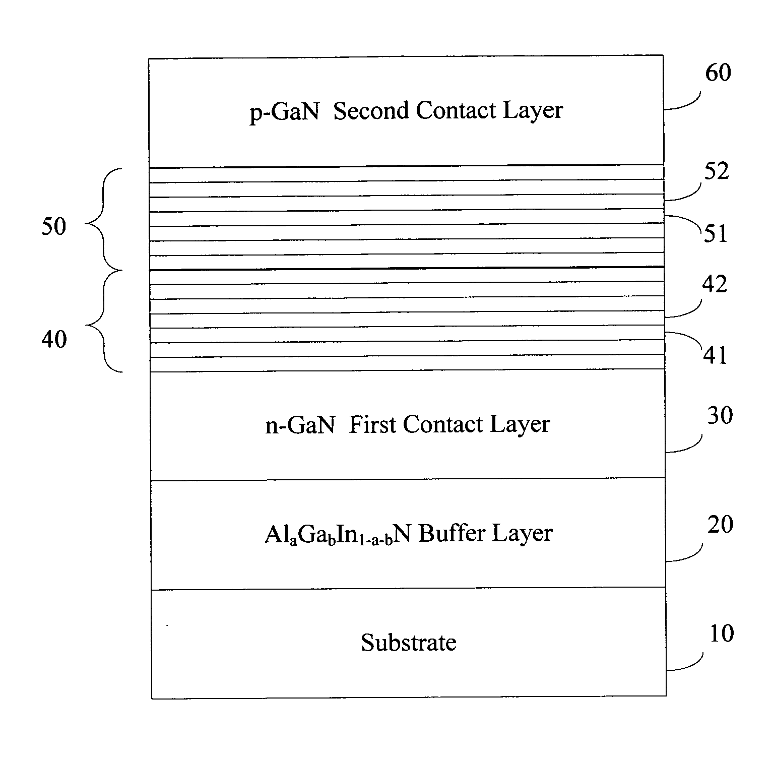
[0017]FIG. 1 is a schematic sectional view showing a nitride based MQW LED structure in accordance with a first embodiment of the present invention. Please note that the present specification uses the term ‘LED structure’ to refer to the epitaxial layer structure of a LED, and the term ‘LED device’ to refer to the semiconductor device obtained from forming the electrodes on a LED structure in a subsequent chip process after the formation of the LED structure.

[0018] As shown in FIG. 1, at the bott...


PUM


Abstract

A MQW LED structure is provided herein, which contains a carrier supply layer joined to a side of the MQW light emitting layer to provide additional carriers for recombination and to avoid / reduce the use of impurity in the light emitting layer. The carrier supply layer contains multiple and interleaving well layers and barrier layers, each having a thickness of 5˜300 Å, with a total thickness of 1˜500 nm. The well layers and the barrier layers are both made of AlpInqGa1-p-qN (p, q≧0, 0≦p+q≦1) compound semiconductor doped with Si or Ge, but with different compositions and with the barrier layers having a higher bandgap than that of the well layers. The carrier supply layer has an electron concentration of 1×10¹⁷˜5×10²¹ / cm3.

Description

BACKGROUND OF THE INVENTION [0001] 1. Field of the Invention [0002] The present invention generally relates to nitride-based multiple quantum-well light emitting diodes, and more particularly to a nitride-based multiple quantum-well light emitting diode having a carrier supply layer to provide additional carriers and to avoid / reduce the use of impurities in the light emitting layer. [0003] 2. The Prior Arts [0004] To enhance the brightness of a gallium nitride-based (GaN-based) light emitting diode (LED), U.S. Pat. No. 5,578,839 teaches a LED structure having a light-emitting layer or an active layer made of InxGa1-xN (0<x<1) compound semiconductor doped with n-typed impurity such as Si and / or with p-typed impurity such as Mg or Zn. The light emitting layer of the LED structure is sandwiched between a first clad layer made of an n-typed GaN-based compound semiconductor and a second clad layer made of a p-typed GaN-based compound semiconductor. The enhanced brightness of the LE...

Claims


Application Information

Patent Timeline
Patent Type & Authority Applications(United States)
IPC IPC(8): H01L33/00H01L33/04H01L33/06H01L33/14H01L33/32
CPCB82Y20/00H01L33/04H01L33/32H01L33/14H01L33/06
Inventor WU, LIANG-WENCHIEN, FEN-REN
Owner FORMOSA EPITAXY INCORPORATION
Why Eureka
Try Eureka