Integrated parallel plate capacitors

a parallel plate capacitor and integrated technology, applied in capacitors, semiconductor devices, semiconductor/solid-state device details, etc., can solve the problems of limited performance of vpp capacitors, extra wafer processing costs of about $25/wafer, etc., to reduce/eliminate additional wiring area, increase capacitance coupling, and improve capacitance density

Active Publication Date: 2007-08-16
IBM CORP
View PDF82 Cites 24 Cited by
  • Summary
  • Abstract
  • Description
  • Claims
  • Application Information

AI Technical Summary

Benefits of technology

[0006] The Mx electrodes are tied together to create a parallel plate capacitor. As a result, the resistance of MIM plates according to the present invention is extremely low, which leads to a high performance MIM capacitor.
[0008] To further enhance capacitance density of this zero-cost high-Q MIM capacitor, Vx vias are added through Mx perforation holes (through-vias). The use of through-vias increases capacitive coupling and reduces / eliminates additional wiring area needed for MIM cap plate connection, which again leads to cap density enhancement.

Problems solved by technology

This additional top plate mask leads to extra wafer processing cost of about $25 / wafer.
However, the performance of a VPP capacitor is limited because of the high resistance associated with metal fingers / vias, which is particularly troublesome for high frequency application.

Method used


Image

  • Integrated parallel plate capacitors
  • Integrated parallel plate capacitors
  • Integrated parallel plate capacitors

Examples


Embodiment Construction

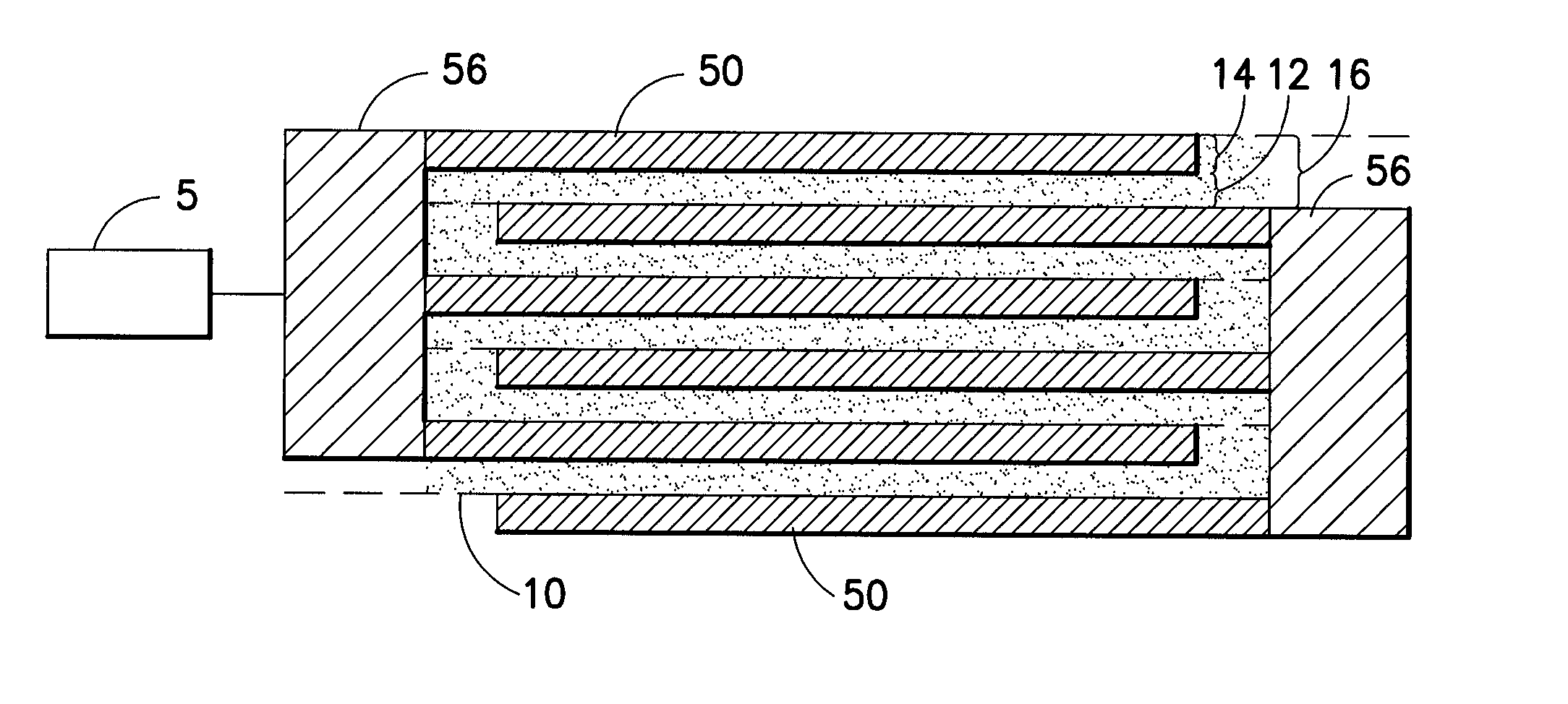
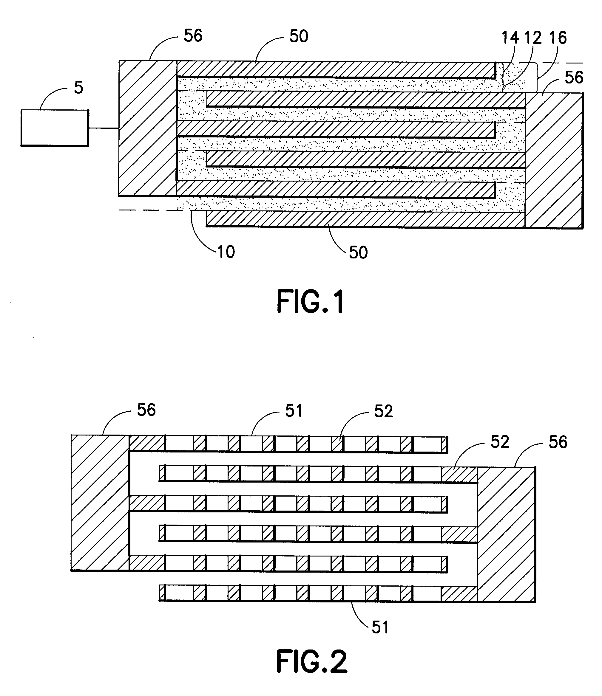
[0016]FIG. 1 shows a set of solid plates 50 connected alternately by vertical connection bars 56. An important feature of this structure compared with prior MIM capacitors is that the thickness 12 of the dielectric between the plates is greater than before because the thickness 12 is the thickness 16 of the back end levels minus the thickness 14 of the interconnects on that back end level; e.g. if the total thickness of the level is 0.5 microns and the thickness of the interconnect on that level is 0.25 microns, then the thickness 12 of the dielectric is also 0.25 microns. Dashed line 10 indicates the top surface of a layer in the back end. A level in the back end containing a capacitor plate will be referred to as a capacitor level. The foregoing means that the capacitance per unit area (capacitance density) is reduced, but that is more than compensated for by the improved reliability provided by the invention. Box 5 represents schematically interconnections on the levels of the BE...


PUM


Abstract

A parallel plate capacitor formed in the back end of an integrated circuit employs conductive capacitor plates that are formed simultaneously with the other interconnects on that level of the back end (having the same material, thickness, etc). The capacitor plates are set into the interlevel dielectric using the same process as the other interconnects on that level of the back end (preferably dual damascene). Some versions of the capacitors have perforations in the plates and vertical conductive members connecting all plates of the same polarity, thereby increasing reliability, saving space and increasing the capacitive density compared with solid plates.

Description

TECHNICAL FIELD [0001] The field of the invention is that of forming a plate capacitor having a set of horizontal conductive plates separated by a dielectric (MIM-CAP). BACKGROUND OF THE INVENTION [0002] High performance (high Q-value) metal-insulator-metal capacitor (MIM cap) is one of the essential passive devices in RF / Analog circuitry. In order to achieve high-Q value, low resistance metal plates are typically used. In prior work, the bottom plate of a metal-insulator-metal (MIM) capacitor is typically made of back end of the line (BEOL) aluminum metal wire on the xth level of the back end (zero-cost). An additional photolithography mask is used for MIM cap top plate formation. This additional top plate mask leads to extra wafer processing cost of about $25 / wafer. In the advanced CMOS technologies with Cu BEOL, up to three masks are employed to create high-Q MIM capacitors. [0003] In an effort to reduce cost, vertical parallel plate capacitors (VPP) have been recently developed / ...

Claims


Application Information

Patent Timeline
Patent Type & Authority Applications(United States)
IPC IPC(8): H01L21/425
CPCH01L23/5223H01L28/60H01L2924/0002H01L2924/00
Inventor COOLBAUGH, DOUGLAS D.DING, HANYIESHUN, EBENEZER E.GORDON, MICHAEL D.HE, ZHONG-XIANGSTAMPER, ANTHONY K.
Owner IBM CORP
Why Eureka
Try Eureka