Charged particle beam projection method and program used therefor

Inactive Publication Date: 2007-08-23
FUJITSU SEMICON LTD
View PDF2 Cites 73 Cited by
  • Summary
  • Abstract
  • Description
  • Claims
  • Application Information

AI Technical Summary

Benefits of technology

[0035] By defining the pattern area density map for each element distribution, it becomes possible to set the small region divided in the pattern area density map to a size suitable for a spread of the element distribution. By d

Problems solved by technology

Patterns to be formed are becoming finer because of recent improvements on an integration degree of semiconductor integrated circuit devices, and a resolution of a conventional optical projection is insufficient nowadays.
On the other hand, it is diff

Method used


Image

  • Charged particle beam projection method and program used therefor
  • Charged particle beam projection method and program used therefor
  • Charged particle beam projection method and program used therefor

Examples


first embodiment

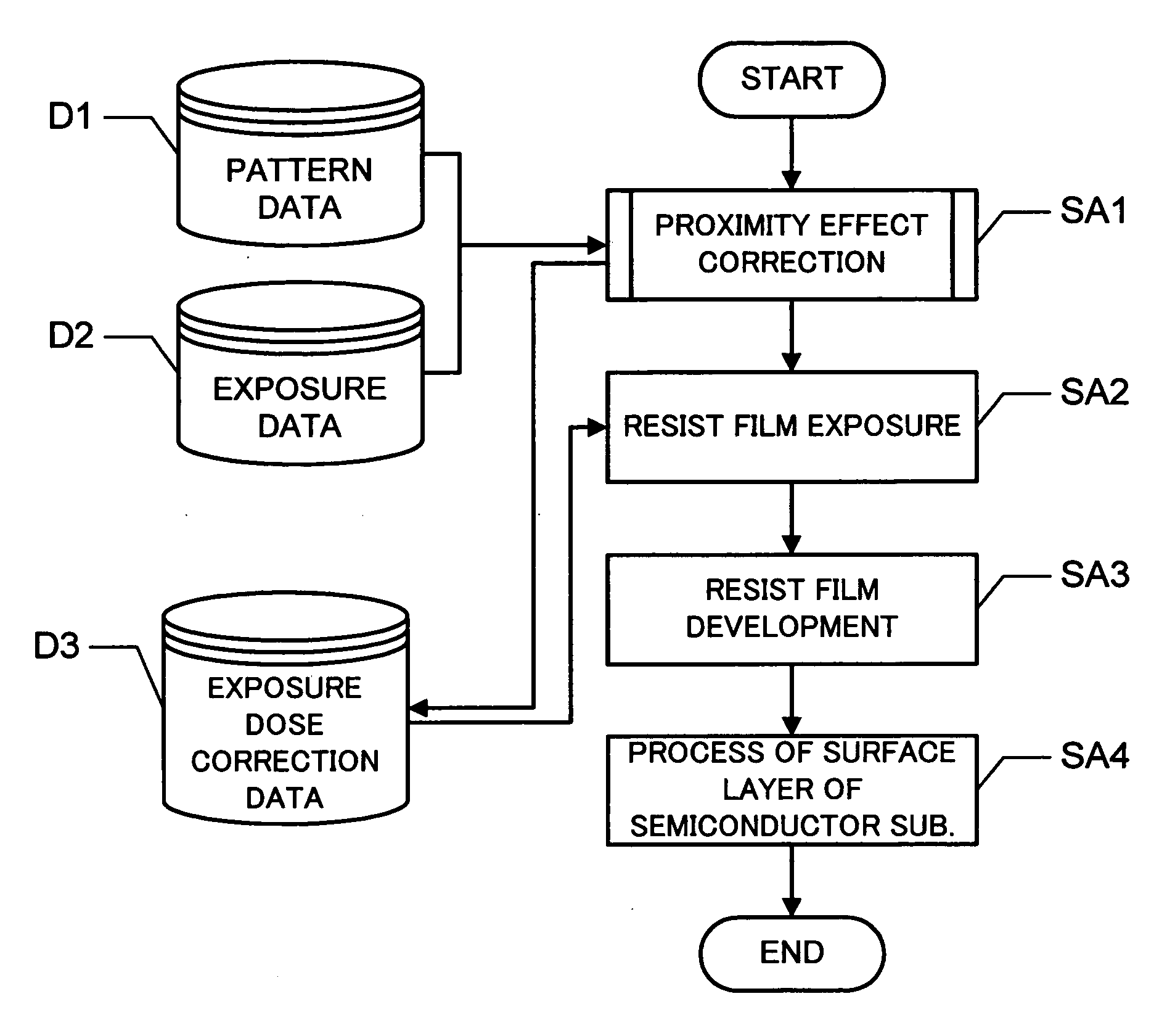
[0048]FIG. 1 is a flow chart illustrating a semiconductor device manufacture method using a projection method according to the Pattern data D1 defines the shape, size, position and the like of a plurality of patterns defined on a pattern layout plane. Exposure data D2 defines a relation between an exposure pattern unit to be exposed by one shot of an electron beam and an exposure dose for the exposure pattern unit. At Step SA1, proximity effect correction is performed by using the pattern data D1 and exposure data D2 to generate exposure dose correction data D3. The exposure dose correction data D3 includes a proper exposure dose assigned to each exposure pattern unit. At Step SA2, a resist film is exposed with an electron beam in accordance with the exposure correction data D3. At Step SA3, the exposed resist film is developed. At Step SA4, a surface layer of the semiconductor substrate is processed by using the developed resist film as a mask.

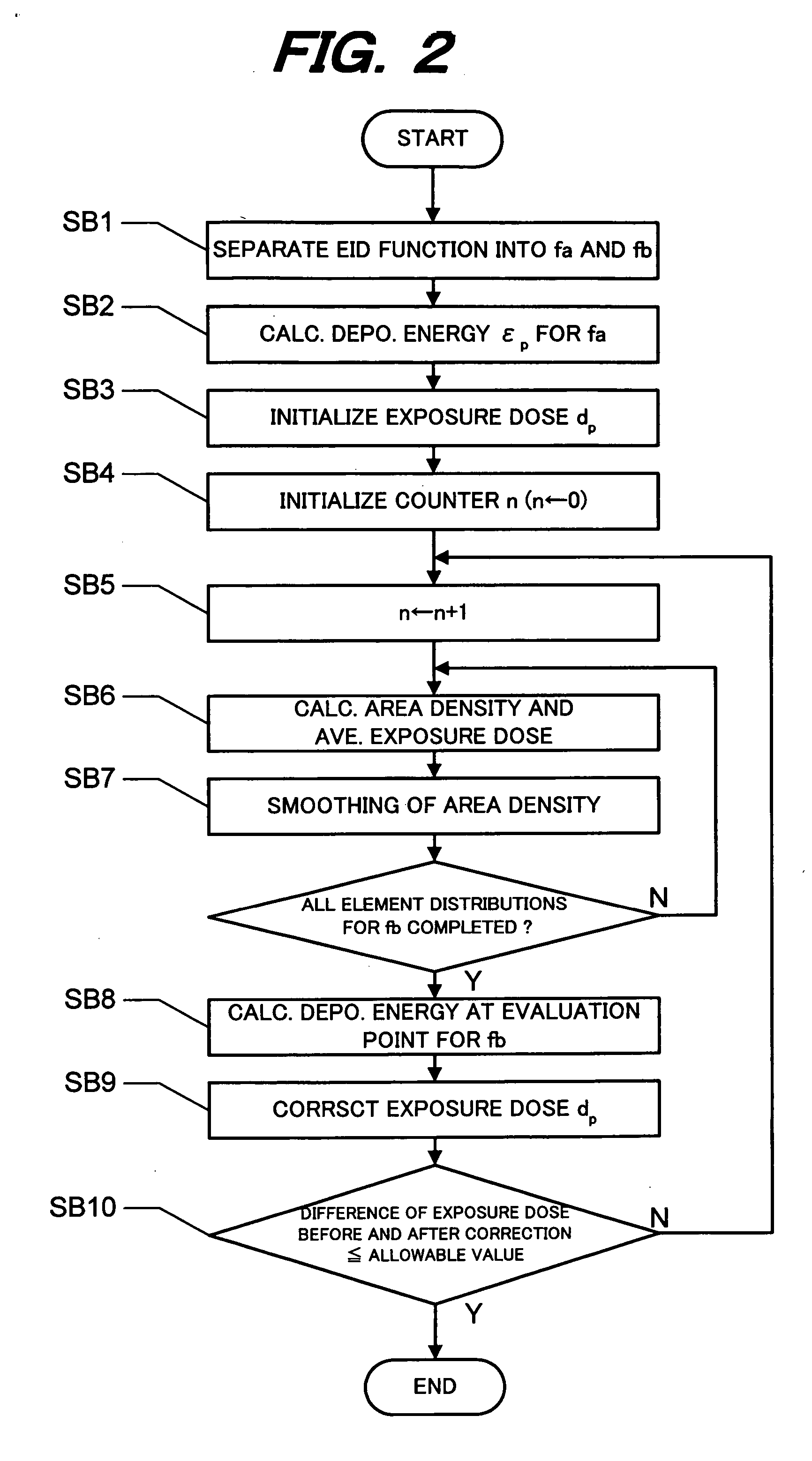
[0049]FIG. 2 is a flow chart illustra...

second embodiment

[0097]FIG. 9 is a flow chart illustrating a semiconductor device manufacture method according to the At Step SC1, a proximity effect correction is conducted by referring to pattern data D1 and exposure data D2 to generate pattern correction data D4. The pattern correction data D4 contains a shift amount of a side of a pattern assigned to each correction unit constituting an exposure pattern. At Step SC2, an exposure mask is formed in accordance with the pattern correction data D4. At Step SC3, a resist film is exposed with an electron beam and developed, by using the formed exposure mask. At Step SC4, a surface layer of the semiconductor substrate is processed by using the developed resist film.

[0098]FIG. 10 is a flow chart illustrating the proximity effect correction process SC1 shown in FIG. 9. In the first embodiment, a proper exposure dose is obtained for each exposure pattern unit, whereas in the second embodiment, the same exposure dose is set to all exposure pattern units, a...

third embodiment

[0113] Prior to describing the third embodiment, description will be directed to a method of calculating a corrected area density disclosed in JP-A-2005-101501. This method takes into consideration the case in which various kinds of materials are distributed on the plane of lower-level layers below the resist film and distribution densities are irregular on the plane.

[0114]FIG. 12 shows a lamination structure of a substrate for which the corrected area density is calculated. A plurality of layers L are formed on a substrate 20, and a resist film 21 is formed as an uppermost layer. The n-th layer as counted from the resist film 21 is represented by L(n). A pattern area density map is defined on the plane of the substrate as in the case of the first and second embodiments.

[0115] A reflection coefficient is represented by rn, corresponding to the number of charged particles transmitted through the layer L(n−1) and reflected by the layer L(n). A transmission coefficient is represented ...


PUM


Abstract

A deposition energy distribution when a charged particle beam is made incident upon a resist film, is approximated by a sum of element distributions having Gaussian distributions. A pattern area density map partitioning the pattern layout plane into small regions, is defined for each element distribution. First and second sub-steps are repeated for each of the pattern area density maps. In the first sub-step, an area density of each small region is obtained. In the second sub-step, in accordance with an energy deposition rate, an exposure dose assigned to a pattern in a first small region, an area of the pattern and the area density of the first small region, the deposition energy to be given to the target small region is obtained and the corrected area density is calculated. A deposition energy at an evaluation point on a pattern layout plane is calculated from the corrected area densities.

Description

CROSS REFERENCE TO RELATED APPLICATION [0001] This application is based on and claims priority of Japanese Patent Applications No. 2006-045739 filed on Feb. 22, 2006, the entire contents of which are incorporated herein by reference. BACKGROUND OF THE INVENTION [0002] A) Field of the Invention [0003] The present invention relates to a projection method using a charged particle beam, and more particularly to a projection method involving proximity effect correction for improving a precision of a pattern size after developing. [0004] B) Description of the Related Art [0005] Patterns to be formed are becoming finer because of recent improvements on an integration degree of semiconductor integrated circuit devices, and a resolution of a conventional optical projection is insufficient nowadays. In order to form a fine pattern, a projection using a charged particle beam, particularly an electron beam, is used. [0006] An electron beam projection method is classified into a point beam proje...

Claims


Application Information

Patent Timeline
IPC IPC(8): G03F7/00
CPCB82Y10/00B82Y40/00H01J37/3174G03F7/2061G03F7/2037
Inventor OGINO, KOZO
Owner FUJITSU SEMICON LTD
Why Eureka
Try Eureka