Nitride semiconductor device and method for fabricating the same

a technology of nitride semiconductor and semiconductor, which is applied in the direction of semiconductor devices, electrical devices, transistors, etc., can solve the problems of difficult to improve the efficiency of light emission from a quantum well, difficult to improve the crystallinity of nitride semiconductor grown on hetero-substrates, and limitations in further intensity and efficiency enhancements. achieve the effect of enhancing intensity and efficiency, reducing spontaneous polarization generation

Active Publication Date: 2007-09-06
PANASONIC CORP
View PDF10 Cites 45 Cited by
  • Summary
  • Abstract
  • Description
  • Claims
  • Application Information

AI Technical Summary

Benefits of technology

[0012]In view of the conventional problems, an object of the present invention is to reduce spontaneous polarization generated in a nitride semiconductor to provide, for example, a light emitting device with enhanced intensity and efficiency, or a field effect transistor with normally-off characteristics.

Problems solved by technology

Initially, it was difficult to improve the crystallinity of the nitride semiconductor grown on the hetero-substrate.
Therefore, for the light emitting device, the quantum-confined Stark effect mentioned above makes it difficult to improve the efficiency of light emission from a quantum well, and thus there are disadvantageous limitations in further intensity and efficiency enhancements.
This disadvantageously makes it difficult to attain the normally-off characteristics.

Method used


Image

  • Nitride semiconductor device and method for fabricating the same
  • Nitride semiconductor device and method for fabricating the same
  • Nitride semiconductor device and method for fabricating the same

Examples


first embodiment

[0065]A first embodiment of the present invention will be described with reference to the accompanying drawings.

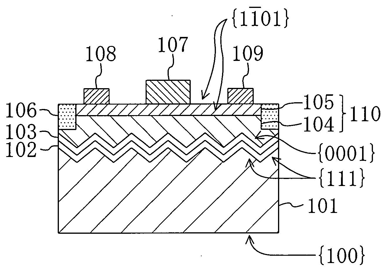
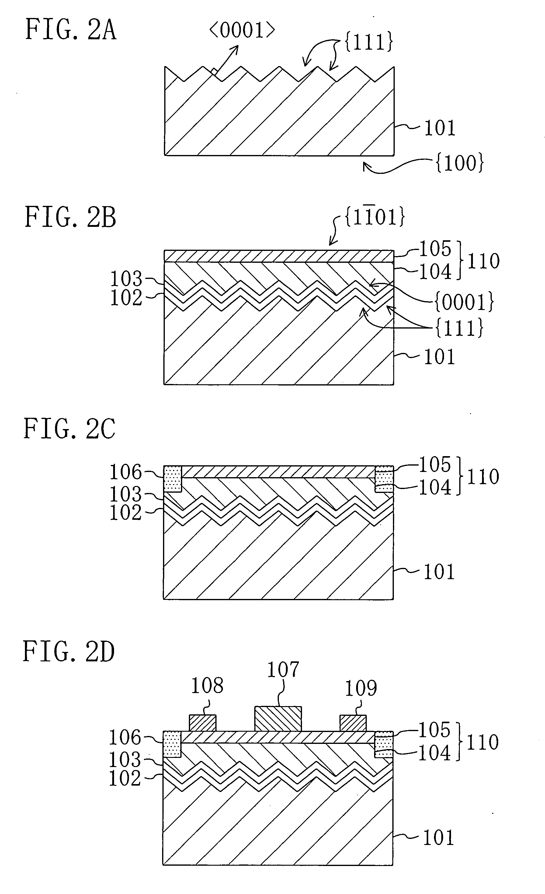
[0066]FIG. 1 is a sectional view of a nitride semiconductor device according to the first embodiment of the present invention, which illustrates a cross-sectional structure of a heterojunction field effect transistor.

[0067]Referring to FIG. 1, a substrate 101 is made of silicon (Si) and has the principal surface with an orientation of {100} plane. On top of the substrate 101, a plurality of indentations composed of a plurality of recesses of V-shaped cross section in a striped arrangement are formed over the entire surface. In this structure, the wall surface of each of the recesses has an orientation of {111} plane of silicon crystal.

[0068]On the indentations of the substrate 101, a buffer layer 102, a superlattice layer 103, a channel layer 104, and a carrier supply layer 105 are sequentially formed by epitaxial growth. The buffer layer 102 is made of aluminum nitride (A...

second embodiment

[0090]A second embodiment of the present invention will be described with reference to the accompanying drawings.

[0091]FIG. 5 is a sectional view of a nitride semiconductor device according to the second embodiment of the present invention, which illustrates a cross-sectional structure of a light emitting diode device.

[0092]Referring to FIG. 5, the GaN-based light emitting diode device according to the second embodiment is formed in the manner in which a holding substrate 301 of, for example, conductive silicon (Si) and a semiconductor stacked structure 210 of a nitride semiconductor are fixed with a p-side electrode 207 and a solder layer 302 containing gold (Au) and tin (Sn). Note that the material for the holding substrate is not limited to silicon, and use can be made of a material capable of further effectively dissipating heat, such as copper tungsten (CuW).

[0093]The semiconductor stacked structure 210 is formed on a growth substrate having been removed (not shown) in the same...


PUM


Abstract

A nitride semiconductor device includes a semiconductor stacked structure which is formed of a nitride semiconductor having a first principal surface and a second principal surface opposed to the first principal surface and which includes an active layer. The first principal surface of the semiconductor stacked structure is formed with a plurality of indentations whose plane orientations are the {0001} plane, and the plane orientation of the second principal surface is the {1-101} plane. The active layer is formed along the {1-101} plane.

Description

CROSS-REFERENCE TO RELATED APPLICATIONS[0001]This application claims priority under 35 U.S.C. § 119 on Patent Application No. 2006-58111 filed in Japan on Mar. 3, 2006, the entire contents of which are hereby incorporated by reference.BACKGROUND OF THE INVENTION[0002](a) Fields of the Invention[0003]The present invention relates to nitride semiconductor devices and their fabrication methods. In particular, the present invention relates to nitride semiconductor devices applicable to field effect transistors or semiconductor light emitting devices and their fabrication methods.[0004](b) Description of Related Art[0005]Gallium nitride (GaN)-based semiconductors (nitride semiconductors) have wider band gaps than compound semiconductors such as gallium arsenide (GaAs) or semiconductors such as silicon (Si). Thus, on the GaN-based semiconductors, active research and development is being carried out toward realization of light emitting devices capable of emitting blue or green visible ligh...

Claims


Application Information

Patent Timeline
Patent Type & Authority Applications(United States)
IPC IPC(8): H01L29/06
CPCH01L29/045H01L29/1029H01L29/2003H01L33/12H01L33/007H01L33/0079H01L33/04H01L29/7787H01L33/0093
Inventor MATSUO, HISAYOSHIMORITA, TATSUOUEDA, TETSUZOUEDA, DAISUKE
Owner PANASONIC CORP
Why Eureka
Try Eureka