

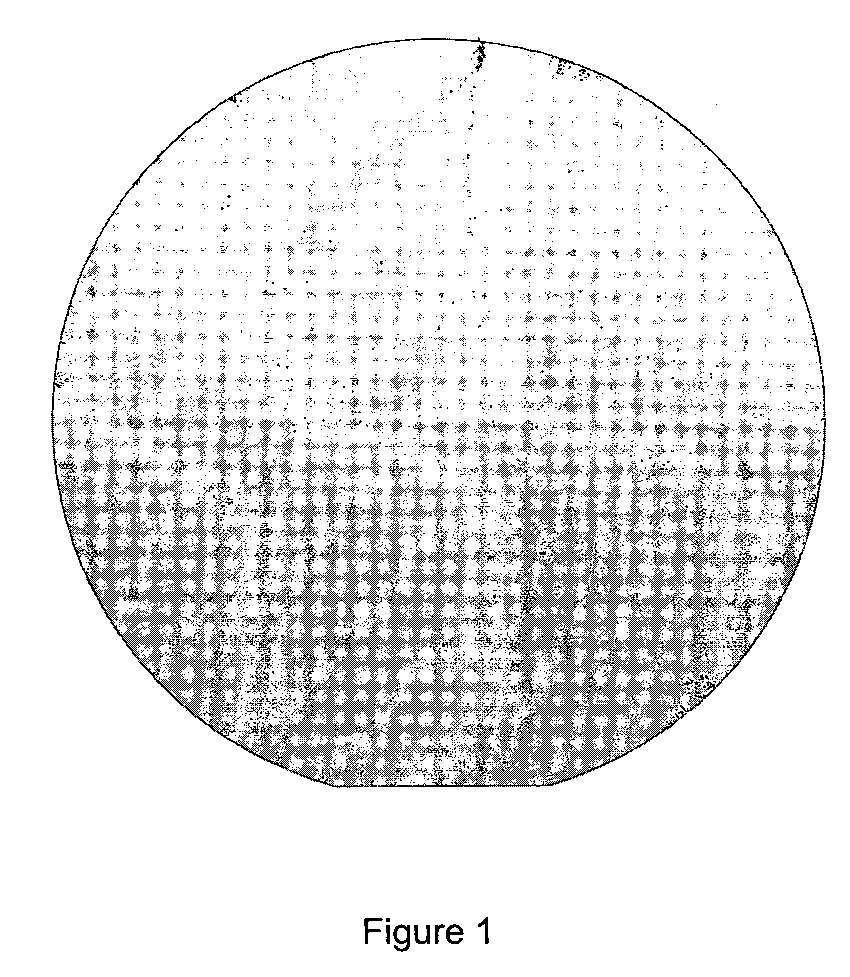
Low micropipe 100 mm silicon carbide wafer
a silicon carbide wafer, low-defect technology, applied in the direction of polycrystalline material growth, crystal growth process, chemically reactive gas, etc., can solve the problem of limiting the performance characteristics of devices made on the substrate, relatively high defect concentration, and constant reduction of structural defects in silicon carbide bulk crystals. problem, to achieve the effect of high quality
Active Publication Date: 2007-09-13
CREE INC
View PDF23 Cites 31 Cited by
- Summary
- Abstract
- Description
- Claims
- Application Information
AI Technical Summary
Benefits of technology
The present invention is a high quality single crystal wafer of silicon carbide (SiC) with a diameter of at least 100 mm and a micropipe density of less than 25 cm−2, which can be used in a seeded sublimation growth system. The invention also includes a method of using this high quality SiC wafer to produce power devices. The technical effects of this invention include improved quality and reliability of SiC wafers for use in power devices, as well as more efficient and reliable production of power devices using SiC wafers.
Problems solved by technology
Although the density of structural defects in silicon carbide bulk crystals has been continually reduced in recent years, relatively high defect concentrations still appear and have been found to be difficult to eliminate, e.g. Nakamura et al., “Ultrahigh quality silicon carbide single crystals,”Nature, Vol. 430, Aug. 26, 2004, page 1009.
These defects can cause significant problems in limiting the performance characteristics of devices made on the substrates, or in some cases can preclude useful devices altogether.
Current seeded sublimation techniques for the production of large bulk single crystals of silicon carbide typically result in a higher than desired concentration of defects on the growing surface of the silicon carbide crystal.
Higher concentrations of defects can cause significant problems in limiting the performance characteristics of devices made on the crystals, or substrates resulting from the crystals.
Thus, the commercial availability of 50 mm (2″) and 75 mm (3″) SiC wafers lags behind these other materials and to some extent limits the adoption and use of SiC in a wider range of devices and applications.
Micropipes are common defects that develop or propagate during the seeded sublimation production of SiC crystals.
Other defects include threading dislocations, hexagonal voids, and screw dislocations.
If these defects remain in the SiC crystal, then resulting devices grown on the crystal may incorporate these defects.
The presence of surface defects in bulk single crystals of SiC may also interfere with single-polytype crystal growth.
The 150 available polytypes of SiC raise a particular difficulty.
Maintaining the desired polytype identity throughout the crystal is only one difficulty in growing SiC crystals of large sizes in a seeded sublimation system.
When surface defects are present, there is not enough polytype information on the crystal surface for depositing layers to maintain the desired polytype.
Polytype changes on the surface of the growing crystal result in the formation of even more surface defects.
Recent research indicates that problems in the bulk crystals produced in a seeded sublimation technique can originate with the seed itself and the manner in which it is physically handled; e.g., Sanchez et al Formation Of Thermal Decomposition Cavities In Physical Vapor Transport Of Silicon Carbide, Journal of Electronic Materials, Volume 29, No. 3, page 347 (2000).
Method used
View moreImage
Smart ImageViewing Examples

Examples
examples
[0058] A series of SiC boules were formed according to the present invention. The micropipe density, as measured by the above-described counting method, of each of these boules is shown in Table 1.
TABLE 1Micropipe Density of SiC boulesBoule NumberMicropipe Density (cm−2)121.82220.21319.97418.42516.67615.96715.6187.23
Login to View More PUM
| Property | Measurement | Unit |
|---|---|---|
| diameter | aaaaa | aaaaa |
| depth | aaaaa | aaaaa |
| temperature | aaaaa | aaaaa |
Abstract
A high quality single crystal wafer of SiC is disclosed having a diameter of at least about 100 mm and a micropipe density of less than about 25 cm−2.
Description
STATEMENT OF GOVERNMENT INTEREST [0001] This invention was developed under Office of Naval Research / DARPA Contract No. N00014-02-C-0306. The government may have certain rights in this invention.BACKGROUND OF THE INVENTION [0002] The present invention relates to low defect Silicon Carbide wafers and their use as precursors for semiconductor purposes, and to seeded sublimation growth of large, high-quality silicon carbide single crystals. [0003] Silicon carbide has found use as semiconductor material for various electronic devices and purposes in recent years. Silicon carbide is especially useful due to its physical strength and high resistance to chemical attack. Silicon carbide also has excellent electronic properties, including radiation hardness, high breakdown field, a relatively wide band gap, high saturated electron drift velocity, high-temperature operation, and absorption and emission of high-energy photons in the blue, violet, and ultraviolet regions of the spectrum. [0004] ...
Claims
Login to View More Application Information
Patent Timeline
 Patent Type & AuthorityApplications(United States)
IPC IPC(8): H01L31/00C30B25/00C01B31/36C30B23/00H01L33/32
CPCC30B23/00H01L29/1608H01L29/04C30B29/36
InventorPOWELL, ADRIANBRADY, MARKLEONARD, ROBERT TYLER
OwnerCREE INC