Wire bonding method for preventing polymer cracking

a technology of polymer and bonding method, which is applied in the direction of electrical apparatus, semiconductor device details, semiconductor/solid-state device devices, etc., can solve the problems of undesirable crack defects in the ic die, limited number of known failure mechanisms,

Active Publication Date: 2007-09-13
QUALCOMM INC
View PDF40 Cites 6 Cited by
  • Summary
  • Abstract
  • Description
  • Claims
  • Application Information

AI Technical Summary

Benefits of technology

[0013]It is one object of the present invention to provide an improved ball-wedge bonding method to solve the prior art problems.

Problems solved by technology

In the past, a large proportion of all semiconductor-device field failures were caused by wire bonds and the number of known failure mechanism were quite limited.
The prior art ball-wedge bonding technology has a drawback in that during wedge boning on the Au pad of an IC die, stress is exerted on the Au pad and the underlying materials layers, inducing undesirable crack defects in the IC die.

Method used


Image

  • Wire bonding method for preventing polymer cracking
  • Wire bonding method for preventing polymer cracking
  • Wire bonding method for preventing polymer cracking

Examples


Embodiment Construction

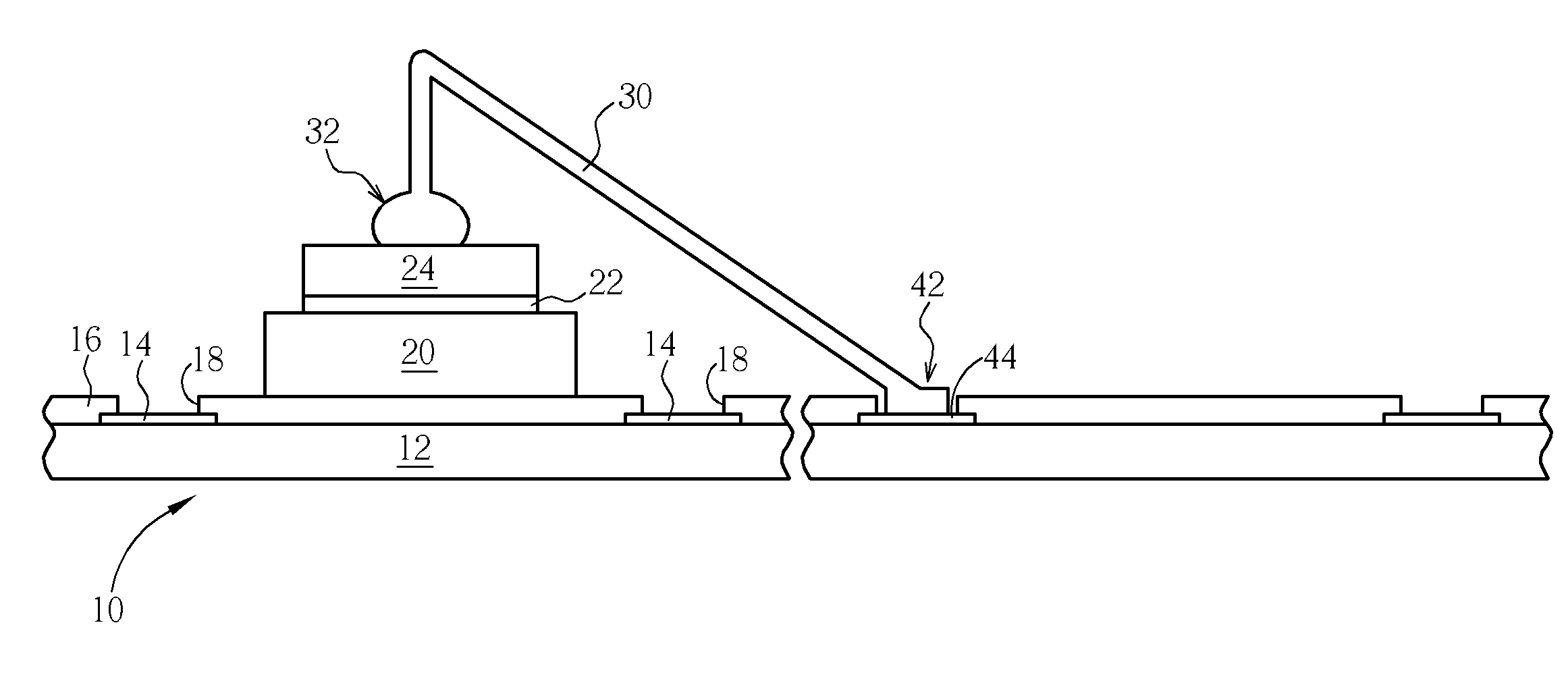
[0026]Please refer to FIG. 1. FIG. 1 is a schematic, cross-sectional diagram illustrating the ball-wedge wire bonding with ball bonding on thick polymer layer in accordance with the first preferred embodiment of this invention.

[0027]As shown in FIG. 1, an integrated circuit (IC) die 10 is provided. The IC die 10 includes active devices and layers of metal interconnection (not shown) that are fabricated in the substrate layer 12. The active devices such as CMOS, BiCMOS devices, transistors, resistors, capacitors, or inductors are fabricated using integrated circuit processes on a semiconductor substrate such as silicon substrate, GaAs substrate or SiGe substrate.

[0028]Multiple inter-layer dielectrics such as low-k dielectric materials, silicon oxide, oxy-nitride are deposited over the semiconductor substrate. The layers of metal interconnection are fabricated in the multiple inter-layer dielectrics by a process comprising sputtering an aluminum layer and then patterning the aluminum ...


PUM

PropertyMeasurementUnit
thicknessaaaaaaaaaa
thicknessaaaaaaaaaa
thicknessaaaaaaaaaa

Abstract

This invention provides a wire bonding method, comprising providing an integrated circuit (IC) die having thereon a passivation layer and a plurality of first bonding pads exposed by respective openings in the passivation layer; forming a polymer layer on the passivation layer; forming an adhesive/barrier layer on the polymer layer; forming a metal pad layer on the adhesive/barrier layer; bonding a wire onto the metal pad layer to form a ball bond thereon; and after forming the ball bond on the metal pad layer, running the wire so as to contact the wire with a second bonding pad and forming a wedge bond thereto.

Description

CROSS REFERENCE TO RELATED APPLICATIONS[0001]This application claims the benefits of U. S. provisional application No. 60 / 743,426, filed Mar. 7, 2006.BACKGROUND OF THE INVENTION[0002]1. Field of the Invention[0003]The present invention relates generally to the field of wire bonding. More particularly, the present invention relates to a ball-wedge bonding process than is capable of preventing polymer such as polyimide cracking.[0004]2. Description of the Prior Art[0005]As known in the art, wire bonding is a technology used to attach a fine wire, usually 1 to 3 mils in diameter, from one connection pad to another, completing the electrical connection in an electronic device. The pads can be bond sites on the semiconductor chip or metallized bond sites on interconnection substrates. Semiconductor die can also be wire bonded to metal lead frames as is done in plastic encapsulated devices.[0006]The methods presently used to wire bond include thermocompression, ultrasonic and thermosonic....

Claims


Application Information

Patent Timeline
Patent Type & Authority Applications(United States)
IPC IPC(8): H01L21/44
CPCH01L24/03H01L24/05H01L24/45H01L24/48H01L24/85H01L2224/04042H01L2224/05073H01L2224/05147H01L2224/05155H01L2224/05157H01L2224/05166H01L2224/05181H01L2224/05639H01L2224/05644H01L2224/05669H01L2224/05673H01L2224/05676H01L2224/45124H01L2224/45144H01L2224/45147H01L2224/48091H01L2224/48227H01L2224/48228H01L2224/4845H01L2224/48465H01L2224/73265H01L2224/78301H01L2224/85045H01L2224/85205H01L2924/01012H01L2924/01013H01L2924/01014H01L2924/01022H01L2924/01025H01L2924/01028H01L2924/01029H01L2924/01047H01L2924/0105H01L2924/01073H01L2924/01075H01L2924/01078H01L2924/01079H01L2924/01082H01L2924/01327H01L2924/04953H01L2924/05042H01L2924/10329H01L2924/14H01L2924/19041H01L2924/19042H01L2924/19043H01L2924/00014H01L2924/01006H01L2924/01019H01L2924/01024H01L2924/01033H01L2924/01044H01L2924/01045H01L2924/01074H01L2224/48644H01L2224/48669H01L2224/48839H01L2224/48844H01L2224/48639H01L2224/48739H01L2224/48769H01L2224/48773H01L2224/48673H01L2224/78H01L2924/00H01L2224/48869H01L2224/48744H01L2224/45015H01L2224/45139H01L2924/15787H01L2224/48873H01L2224/85203H01L24/49H01L2224/48137H01L2224/48247H01L2224/48257H01L2224/4903H01L2224/85H01L2924/00011H01L2924/00015H01L2924/20752H01L2924/20753H01L2924/20754H01L2924/20755H01L2924/20756H01L2924/20757H01L2924/01049
Inventor CHOU, CHIU-MINGLIN, SHIH-HSIUNGLIN, MOU-SHIUNGLO, HSIN-JUNG
Owner QUALCOMM INC
Why Eureka
Try Eureka