
Tuneable semiconductor device

a semiconductor device and a technology of tunable semiconductors, applied in semiconductor devices, transistors, electrical devices, etc., can solve the problems of high avalanche multiplication, reduced collector-emitter breakdown voltage (bvceo), and increased processing costs

Inactive Publication Date: 2007-09-20
GLOBALFOUNDRIES INC
View PDF10 Cites 13 Cited by
  • Summary
  • Abstract
  • Description
  • Claims
  • Application Information

AI Technical Summary

Benefits of technology

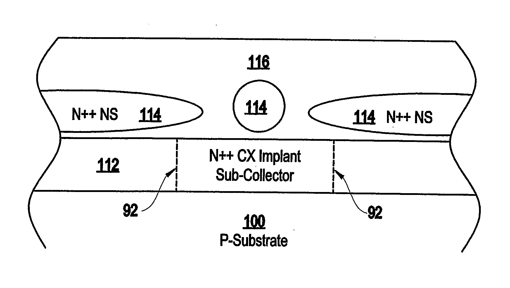
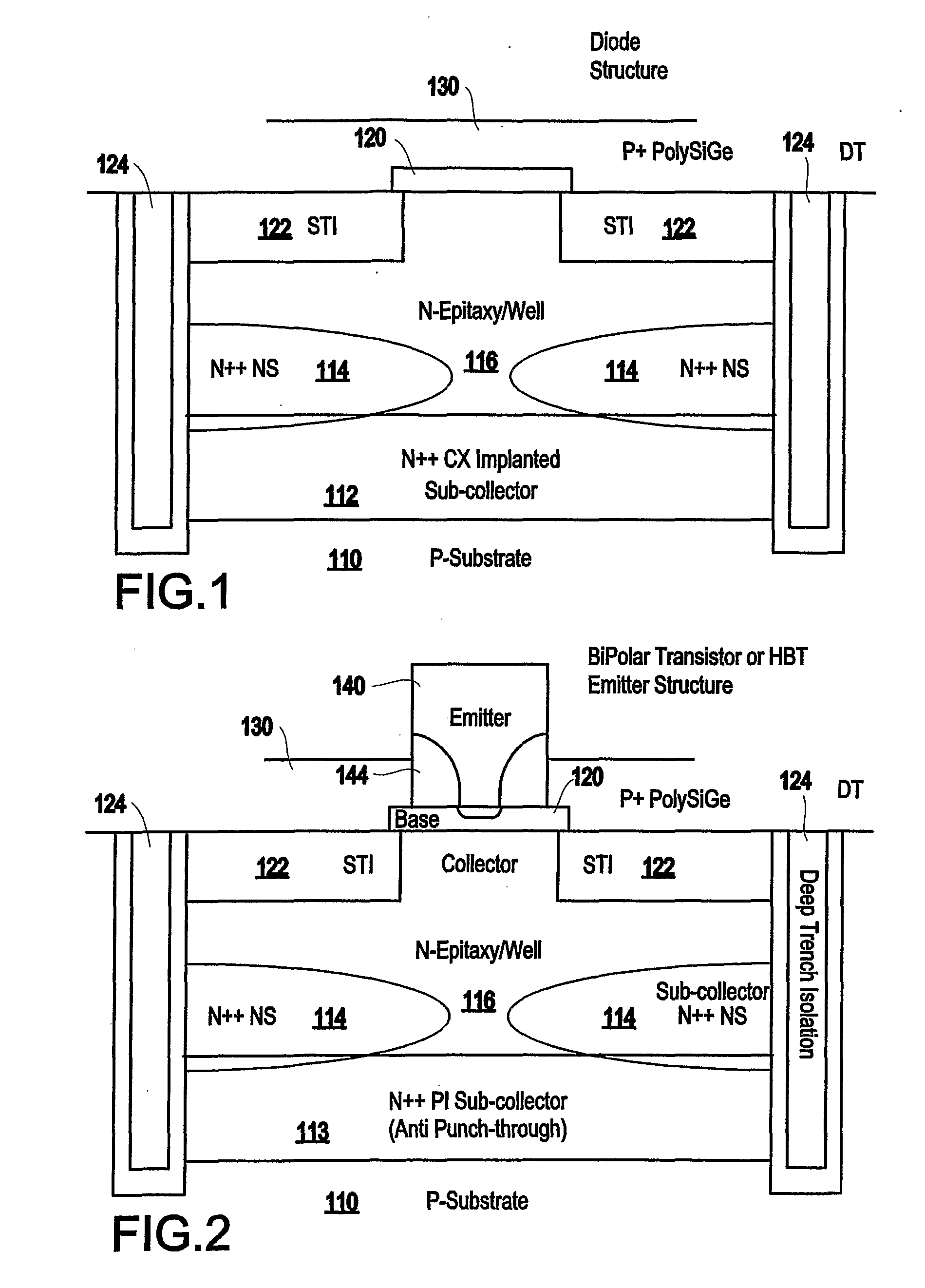
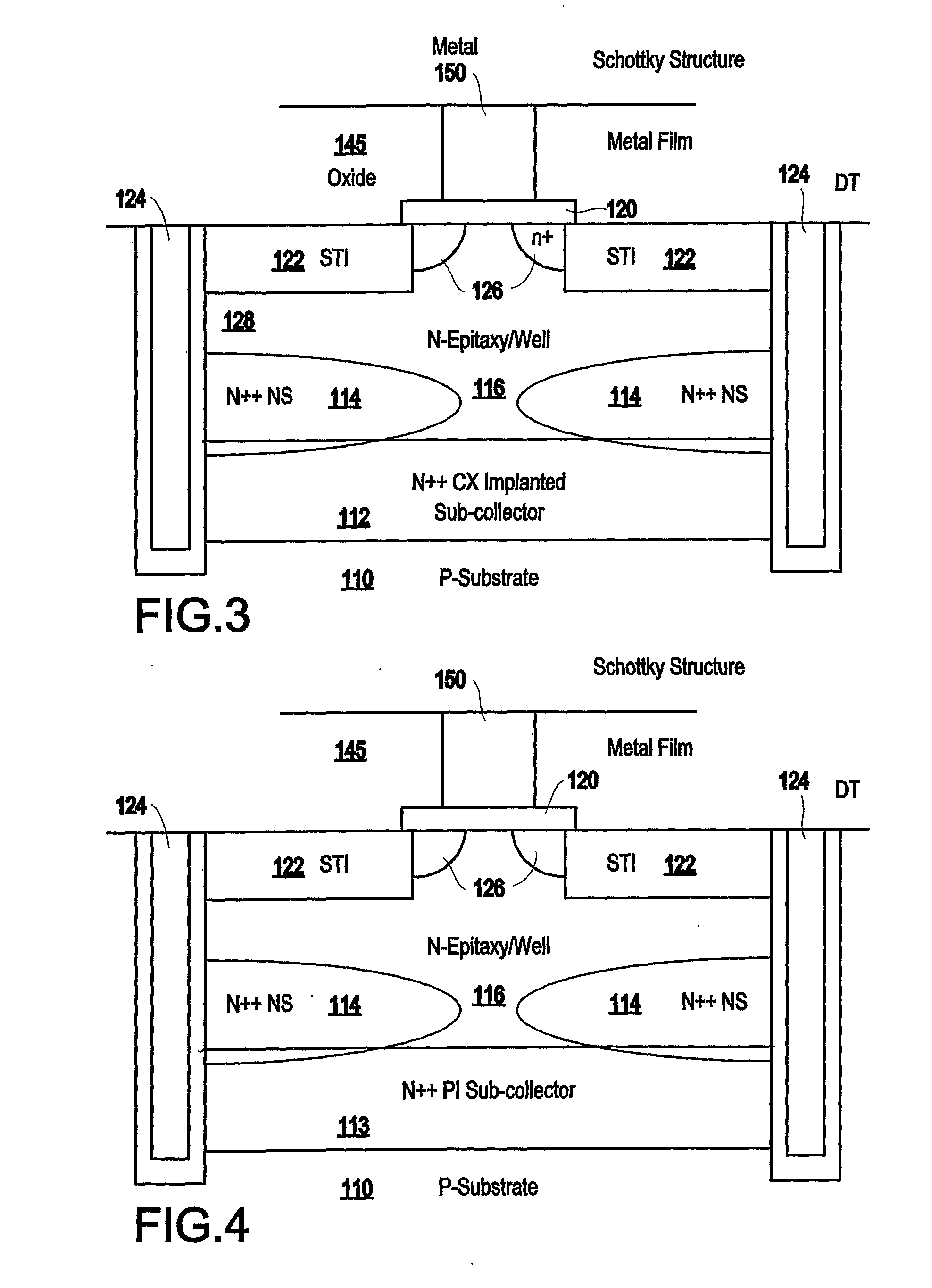
The invention is a semiconductor structure that includes a discontinuous non-planar sub-collector with a different polarity than the underlying substrate. The structure also includes an active area, a base, and an emitter. The distance between the discontinuous portions of the sub-collector tunes the performance characteristics of the semiconductor structure. The sub-collector has a higher impurity concentration and non-planar upper and lower surfaces. The invention provides a method of forming the semiconductor structure by epitaxially growing the collector on the substrate. The process expands the second discontinuous sub-collector and automatically provides doping to the collector. The technical effects of the invention include improved performance and reliability of semiconductor devices.

Problems solved by technology

These processes all add additional cost to the technology.
Additionally, with epitaxial elimination, sub-collectors are required to be implanted due to limitation on the high energy implanter and dose throughput at higher energies.
However, no matter what selectively implanted collector profile is used, as the vertical profile is scaled, electric fields between the base and sub-collector increase, resulting in higher avalanche multiplication and eventually to a lower collector-emitter breakdown voltage (BVceo).
This pedestal implant requires an additional implant process step and adds cost to a semiconductor process.
This leads to higher collector sheet resistances, and lower unity power gain cutoff frequency (fMAX).
As a result, the scaling of the vertical profile leads to a higher injection into the substrate wafer, which can increase the noise in adjacent circuitry or elements.
The increase in the minority carrier injection into the substrate can also lead to latchup.

Method used


Image

  • Tuneable semiconductor device
  • Tuneable semiconductor device
  • Tuneable semiconductor device

Examples


Embodiment Construction

[0035] The present invention and the various features and advantageous details thereof are explained more fully with reference to the non-limiting embodiments that are illustrated in the accompanying drawings and detailed in the following description. It should be noted that the features illustrated in the drawings are not necessarily drawn to scale. Descriptions of well-known components and processing techniques are omitted so as to not unnecessarily obscure the present invention. The examples used herein are intended merely to facilitate an understanding of ways in which the invention may be practiced and to further enable those of skill in the art to practice the invention. Accordingly, the examples should not be construed as limiting the scope of the invention.

[0036] The invention overcomes the high breakdown device problem discussed above by masking the doping of the sub-collector under the active area 116 of the HB device to form discontinuous sub-collector regions. The inven...


PUM


Abstract

Disclosed is a method of forming a semiconductor structure that includes a discontinuous non-planar sub-collector having a different polarity than the underlying substrate. In addition, this structure includes an active area (collector) above the sub-collector, a base above the active area, and an emitter above the base. The distance between the discontinuous portions of the discontinuous sub-collector tunes the performance characteristics of the semiconductor structure. The performance characteristics that are tunable include breakdown voltage, unity current gain cutoff frequency, unity power gain cutoff frequency, transit frequency, current density, capacitance range, noise injection, minority carrier injection and trigger and holding voltage.

Description

BACKGROUND OF THE INVENTION [0001] 1. Field of the Invention [0002] The present invention generally relates to various semiconductor structures and more particularly to an improved structure that includes improved sub-collector areas that have non-planar surfaces. [0003] 2. Description of the Related Art [0004] With mixed voltage interface (MVI) applications, the desire to have multiple MOSFET (Metal Oxide Semiconductor Field Effect Transistor) devices and multiple bipolar transistors in CMOS (Complementary Metal Oxide Semiconductor) and BiCMOS (Bipolar CMOS) technologies is common practice. It is also common practice in CMOS to have thin oxide, and dual oxide MOSFET devices to provide this capability. Additionally, in BiCMOS technology, both a high breakdown (HB) and high performance (HP) BJT (Bipolar Junction Transistor) (or HBT) device is desirable for mixed voltage applications that require both high voltage interfaces as well as performance requirements. The addition of multipl...

Claims


Application Information

Patent Timeline
Patent Type & Authority Applications(United States)
IPC IPC(8): H01L29/66H01L21/331H01L21/332H01L29/00H01L29/08H01L29/737H01L29/74H01L29/861H01L29/872H01L29/93
CPCH01L29/0821H01L29/0834H01L29/66242H01L29/66363H01L29/93H01L29/74H01L29/861H01L29/872H01L29/7378H01L29/73
Inventor STRICKER, ANDREASSHERIDAN, DAVIDRIEH, JAE-SUNGFREEMAN, GREGVOLDMAN, STEVENONGE, STEPHEN A.ST.
Owner GLOBALFOUNDRIES INC
Learn More