Top-emitting OLED device with improved stability

a technology of organic light and diodes, which is applied in the direction of organic semiconductor devices, discharge tubes/lamp details, discharge tubes luminescnet screens, etc., can solve the problems of large amount of generated light trapped within the device, large display area on the substrate is not available for light to emerge, and small fraction of generated light is available for viewing, etc., to achieve improved long-term operational stability, increase lateral electrical conductivity, and high yield

Inactive Publication Date: 2007-09-27
EASTMAN KODAK CO
View PDF3 Cites 34 Cited by
  • Summary
  • Abstract
  • Description
  • Claims
  • Application Information

AI Technical Summary

Benefits of technology

[0015] It is therefore an object of the present invention to provide a top-emitting OLED device (TE-OLED) with improved long-term operational stability. Another object of the present invention is to provide a device capable of being manufactured with high yield. It is a further object of this invention to provide a cathode with increased lateral electrical conductivity for improved a real uniformity of luminance.

Problems solved by technology

However, only a small fraction of generated light is available for viewing, and about 80% of generated light is trapped within the device in waveguiding modes in glass, ITO and organic layers.
Consequently the entire display area on the substrate is not available for the light to emerge.
To compensate for the reduced average brightness level the drive current has to be increased subjecting the display to increased risk of operational degradation.
It follows that further improvement in back plane design cannot be readily implemented without further compromising the aperture ratio and the operational stability.
However, realizing high efficiency by reclaiming light lost to waveguiding modes can be very difficult.
To recover even a fraction of light lost to the waveguiding modes the device architecture can be very complex.
One of the disadvantages of an Ag cathode is the unpredictability of device yield and irreproducibility of device characteristics.
The devices that initially work often fail in operation.
The modes of failure include rapid performance degradation and catastrophic failure.
In the catastrophic mode the luminescence vanishes unpredictably and instantly.
However, reactivity of Ag is high and its adhesion is low.
The interface between the organic and Ag can be incomplete and unstable defects can exist.
With the existence of these defects paths are generated in addition to normal carrier path resulting in a leaky or short-circuited diode.
The leaky diodes are believed responsible for catastrophic failures in operation.
Another problem associated with thin electrode is that the film is not robust.
However, the sputtering deposition of the capping layer on the thin Ag layer increases the occurrence of short circuits between the anode and the cathodes causing further reduction of device yields.
However Al is not generally considered suitable because of expected low efficiency due to high absorptivity of Al.
Even with higher enhancement of top-emission with a capping layer the semitransparent Al electrode devices may still not be as efficient as the device that uses Ag as the semitransparent electrode.
The electrode structure involving Al can be unstable if the capping layer is not properly selected.
In extended operation the In and Sn can diffuse through the cathode and eventually creating electrical shorts between the anode and the cathode causing complete failure of the device.
As Al is very reactive to many oxides, nitrides and other compounds that included in the transparent capping layer, the electrode structure can be unstable.

Method used


Image

  • Top-emitting OLED device with improved stability
  • Top-emitting OLED device with improved stability
  • Top-emitting OLED device with improved stability

Examples


Embodiment Construction

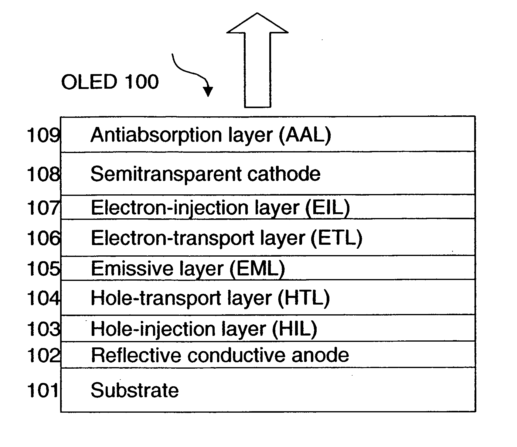
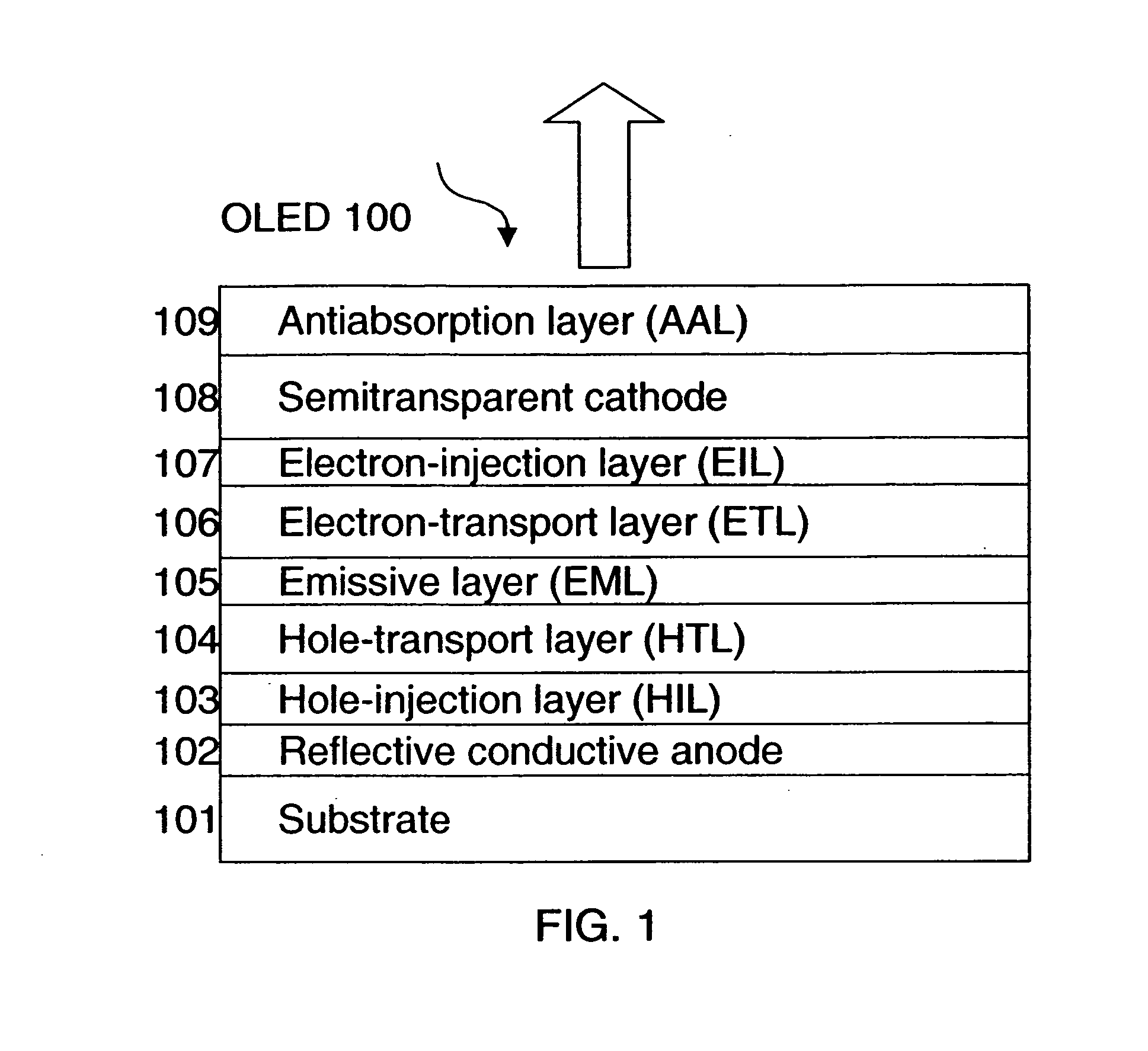
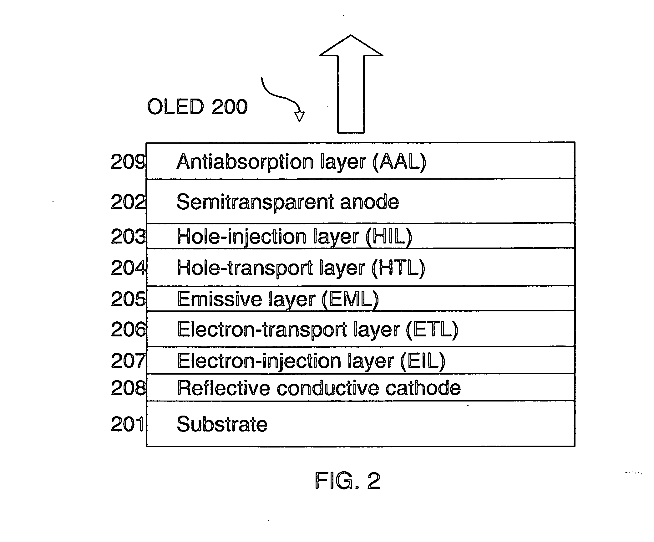
[0024] Throughout the ensuing description acronyms are used to designate the names of the different organic layers and operating features of organic light-emitting devices. For reference they are listed in Table 1.

TABLE 1OLEDOrganic light-emitting diodeITOIndium tin oxideIZOIndium zinc oxideHILHole- injection LayerHTLHole-transport layerEMLEmissive layerETLElectron-transport layerEILElectron injection layerAALAnti-absorption layerARLAbsorption reduction layerNPB4,4′-Bis[N-(1-naphthyl)-N-phenylamino]biphenyl (NPB)AlqTris(8-hydroxyquinoline) aluminumTCOTransparent conductive oxide

[0025] Turning to FIG. 1, the OLED 100 is a top-emitting OLED device of the present invention, which includes a reflective and conductive anode 102, a hole-injection layer (HIL) 103, a hole-transport layer (HTL) 104, an emissive layer (EML) 105, an electron-transport layer (ETL) 106, an electron-injection layer (EIL) 107, a semitransparent cathode 108, and an anti-absorption layer (AAL) 109 successively dis...


PUM

PropertyMeasurementUnit
work functionaaaaaaaaaa
thicknessaaaaaaaaaa
thicknessaaaaaaaaaa

Abstract

A top-emitting OLED device including a substrate; a reflective and conductive first electrode including a metal or metal alloy or both formed over the substrate; at least one organic layer formed over the first electrode and including an emissive layer having electroluminescent material; and a semitransparent, reflective and conductive second electrode provided over the organic layer, wherein the second electrode includes a first layer having material M, wherein M is a metal, and a second layer providing an anti-absorption function in contact with the first layer and having a compound M′X , wherein M′ is a ‘metal and X is a non-metal, wherein M′X has a free energy of formation [equal to or ]more negative than the free energy of formation of MX.

Description

FIELD OF THE INVENTION [0001] The present invention relates to a top-emitting organic light-emitting diode device having metallic electrodes with improved reliability and enhanced operational stability. BACKGROUND OF THE INVENTION [0002] An organic electroluminescent (OEL) device, alternately known as organic light emitting diode (OLED), is useful in flat-panel display applications. This light-emissive device is attractive because it can be designed to produce red, green, and blue colors with high luminance efficiency; operable with a low driving voltage on the order of a few volts, and clearly viewable from oblique angles. These unique attributes are derived from a basic OLED structure including a multilayer stack of thin films of small-molecule organic materials sandwiched between an anode and a cathode. Tang et al in commonly-assigned U.S. Pat. Nos. 4,769,292 and 4,885,211 disclose such a structure. The common electroluminescent (EL) medium includes a bilayer structure of a hole-...

Claims


Application Information

Patent Timeline
Patent Type & Authority Applications(United States)
IPC IPC(8): H01J1/62H01J63/04
CPCH01L51/5088H01L51/5206H01L2251/5315H01L51/5265H01L51/5234H10K50/17H10K50/816H10K50/818H10K50/828H10K50/852H10K2102/3026
Inventor RAYCHAUDHURI, PRANAB K.MADATHIL, JOSEPH K.SHORE, JOEL D.
Owner EASTMAN KODAK CO
Why Eureka
Try Eureka