Semiconductor processing with a remote plasma source for self-cleaning

a plasma source and semiconductor technology, applied in chemical vapor deposition coatings, coatings, chemistry apparatuses and processes, etc., can solve problems such as increased operation costs, damage to the surface of electrodes, and defects in manufactured semiconductor circuits

Inactive Publication Date: 2007-10-04
ASM JAPAN
View PDF44 Cites 169 Cited by
  • Summary
  • Abstract
  • Description
  • Claims
  • Application Information

AI Technical Summary

Benefits of technology

[0027] The skilled artisan will readily appreciate in view of the present disclosure that, while each of features (a), (b), and (c) are advantageous in and of themselves, combining two or all of (a), (b) and (c) will synergistically enhance the advantageous effects.

Problems solved by technology

This causes impurity contamination that leads to defects in manufactured semiconductor circuits.
As a result, the surface of electrodes is damaged; a surface layer comes off to cause impurity contamination.
It becomes necessary to replace damaged parts frequently, which increases operation cost.

Method used


Image

  • Semiconductor processing with a remote plasma source for self-cleaning
  • Semiconductor processing with a remote plasma source for self-cleaning
  • Semiconductor processing with a remote plasma source for self-cleaning

Examples


embodiment 1

Main Structures

[0071] A first embodiment will be explained with reference to FIG. 1.

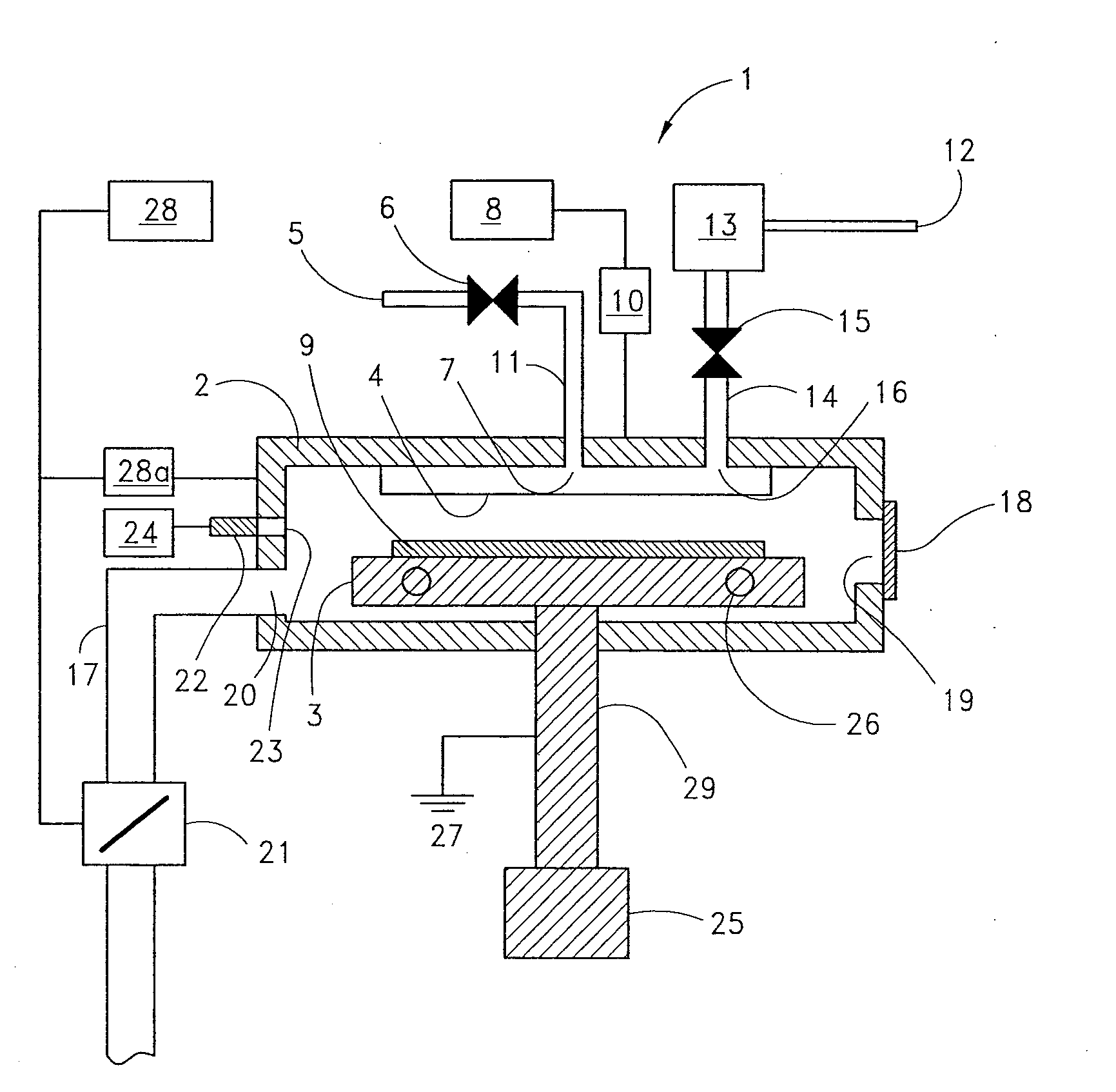
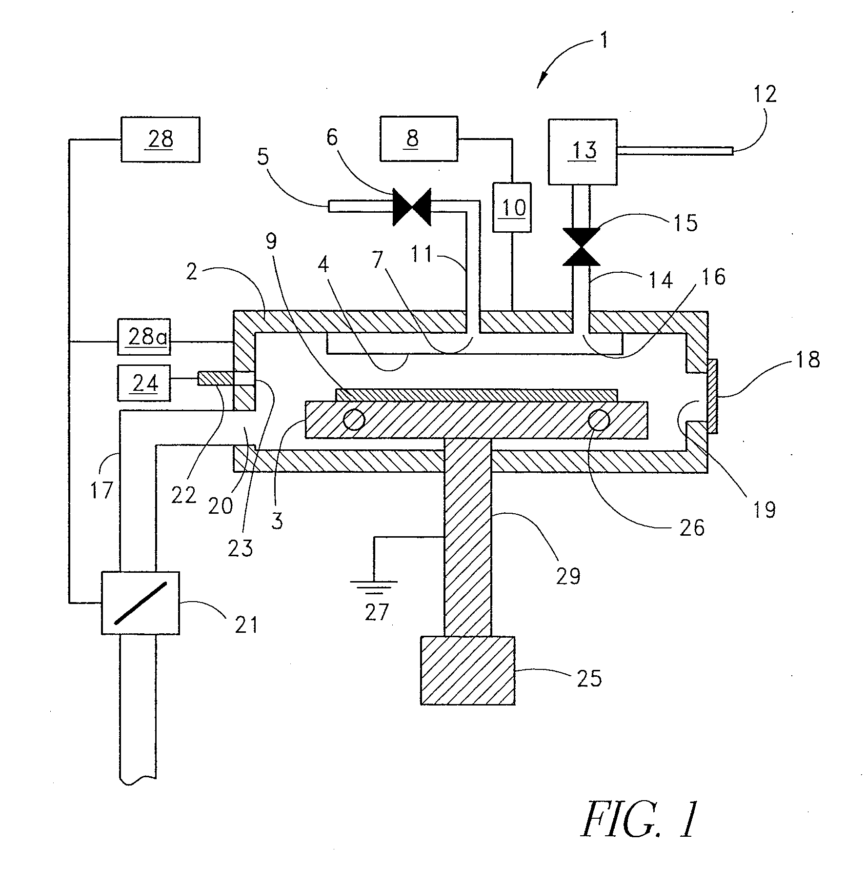
[0072]FIG. 1 is a schematic cross section of an exemplary a plasma CVD device according to this embodiment. A plasma CVD device 1, which is used to form a thin film on a semiconductor wafer 9 or other substrate, comprises a reaction chamber 2, a support 3 provided within the reaction chamber to support the semiconductor wafer 9, a showerhead 4 that is positioned to face the support 3 and is used to jet out reaction gas uniformly onto the semiconductor wafer 9, an outlet 20 to exhaust reaction gases and byproducts from the reaction chamber 2, and a remote plasma discharge chamber 13. The remote plasma discharge chamber 13 is positioned remotely from reaction chamber 2 and is linked to the showerhead 4 via piping 14 and valve 15. The remote plasma discharge chamber 13 has characteristics wherein it generates active species using radio-frequency oscillating output energy of the designated frequency a...

embodiment 2

Structures

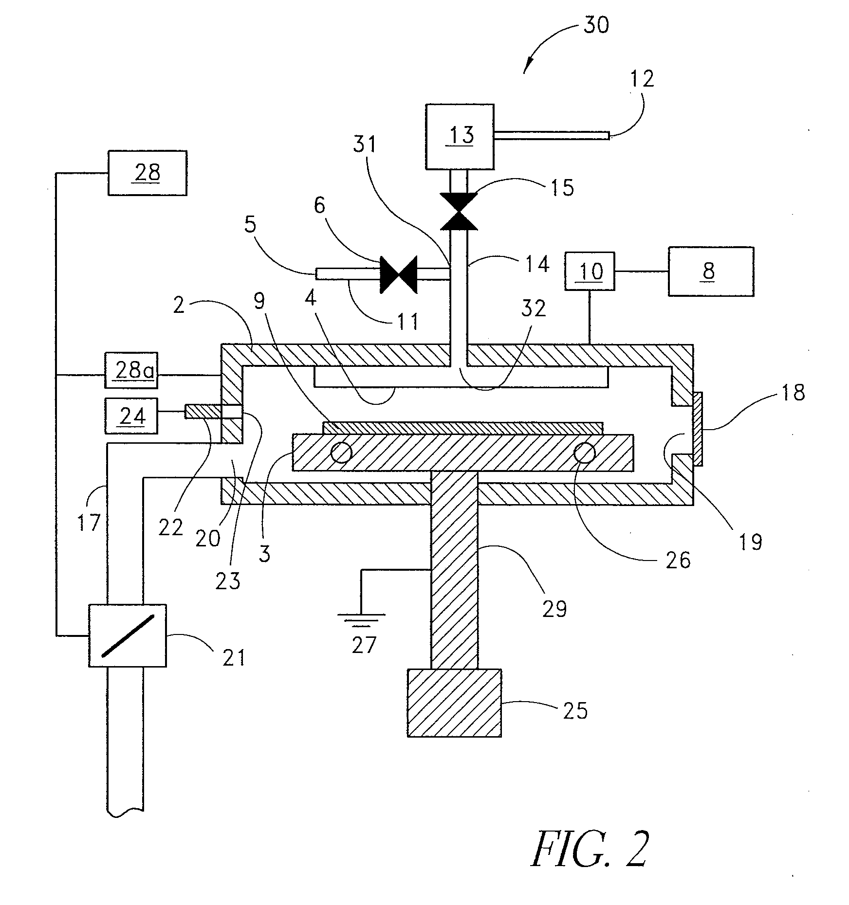
[0091]FIG. 2 shows another example according to this embodiment. Unlike the plasma CVD device 1 of FIG. 1, a plasma CVD device 30 of FIG. 2 includes a link between one end of the reaction conduit 11 and piping 14 at abjection 31 positioned between the remote plasma discharge chamber 13 and a gas exit port 32. Reaction gas and cleaning gas are mixed at the junction 31 and are brought into a showerhead 4 from one gas inlet port 32. The device 30 can be otherwise similar to the device 1 of FIG. 1.

[0092] In the illustrated example, the valve 15 is set up at the plasma discharge chamber side before the junction 31. For the internal surface of the piping 14 and the valves 6, 15, preferably fluorine-passivated aluminum, aluminum alloy, stainless steel or nickel material is used, but aluminum or aluminum alloy can also be used. For sealing materials of the valves 6, 15, preferably fluorocarbon polymers such as PTFE (polytetrafluoroethylene), PFA (tetrafluoroethylene·perfluoroal...

embodiment 3

Main Structures

[0095]FIG. 3 is a schematic diagram showing a cross sectional view of a preferable implementation example of a plasma CVD device according to this embodiment. A plasma CVD device 1, which is used to form a thin film on a semiconductor wafer 9 or other substrate, comprises a reaction chamber 2, a support 3 provided within the reaction chamber 2 to place the semiconductor wafer 9, a showerhead 4 that positioned facing the support 3 and is used to inject reaction gas uniformly onto the semiconductor wafer 9, an outlet 20 to exhaust the inside of reaction chamber 2. The remote plasma discharge chamber 13 is positioned remotely from reaction chamber 2 and is linked to the showerhead 4 via piping 14 and valve 15. The remote plasma discharge chamber 13 has characteristics wherein it generates active species using radio-frequency oscillating output energy of the designated frequency.

[0096] On one side of the reaction chamber 2, an opening 19 is formed and the reaction cham...


PUM

PropertyMeasurementUnit
frequencyaaaaaaaaaa
frequencyaaaaaaaaaa
diameteraaaaaaaaaa

Abstract

A plasma CVD device includes a reaction chamber, a remote plasma discharge chamber that is provided remotely from the reaction chamber, and piping that links the reaction chamber and the remote plasma discharge chamber. The remote plasma discharge chamber activates cleaning gas by plasma discharge energy, and the activated cleaning gas is introduced into the inside of the reaction chamber through the piping and changes solid substances that adhere to the inside of the reaction chamber in consequence of film formation, to gaseous substances, thereby cleaning the inside of the reaction chamber. The device is characterized by at least one of the following: (a) the remote plasma discharge chamber generates active species using radio frequency oscillating output energy of a preselected frequency; (b) the piping is made of materials that are not corroded by the active species; or (c) the piping is provided with a through-flow type valve.

Description

REFERENCE TO RELATED APPLICATION [0001] The present application is a continuation of U.S. application Ser. No. 10 / 759,925, filed Jan. 16, 2004, which is a continuation of U.S. application Ser. No. 09 / 764,523, filed Jan. 18, 2001, now issued as U.S. Pat. No. 6,736,147, and which claims the priority benefit of U.S. provisional application No. 60 / 176,592, filed Jan. 18, 2000. The entirety of U.S. application Ser. No. 10 / 759,925 is incorporated herein by reference.BACKGROUND OF THE INVENTION [0002] 1. Field of the Invention [0003] This invention relates to a CVD (chemical vapor deposition) device equipped with a self-cleaning device. In particular, the invention relates to a device that cleans the inside of a deposition chamber using remotely generated active species. [0004] 2. Description of the Related Art [0005] CVD devices have been conventionally used to form insulation films such as silicon oxide, silicon nitride, amorphous carbon or polymer containing benzene ring, conductor film...

Claims


Application Information

Patent Timeline
Patent Type & Authority Applications(United States)
IPC IPC(8): C25F1/00C23C16/44C23C16/452H01J37/32H01L21/205H01L21/302H01L21/3065
CPCC23C16/4405H01J37/32862H01J37/32357C23C16/452C23C16/50
Inventor SATOH, KIYOSHISATO, KAZUOFUKUDA, HIDEAKI
Owner ASM JAPAN
Why Eureka
Try Eureka