Nonvolatile semiconductor memory device and manufacturing method thereof

a nonvolatile, memory device technology, applied in semiconductor devices, semiconductor/solid-state device details, electrical devices, etc., can solve the problems of reducing the reliability of the nonvolatile semiconductor memory device, the edge of the semiconductor layer cannot be sufficiently covered with an insulating layer, and the thermal oxidation method is difficult to use, so as to reduce the influence of an edge of a channel formation region of the semiconductor layer, improve reliability, and reduce the effect of reading defects

Inactive Publication Date: 2007-10-04
SEMICON ENERGY LAB CO LTD
View PDF5 Cites 41 Cited by
  • Summary
  • Abstract
  • Description
  • Claims
  • Application Information

AI Technical Summary

Benefits of technology

[0015]In a nonvolatile semiconductor memory device, when a first insulating layer which can serve as a tunnel insulating film is formed by high density plasma treatment, defects inside the film can be reduced and reliability can be improved (writing defects or reading defects can be reduced). In addition, in the nonvolatile semiconductor memory device, when an impurity region having a different conductivity type from that of a source region or drain region is provided in a region which is an edge of the semiconductor layer and overlaps with a control gate electrode, influence due to an edge of a channel formation region of the semiconductor layer can be reduced.

Problems solved by technology

In general, in the case of forming a nonvolatile semiconductor memory device over a substrate with low heat resistance, such as glass, with the use of an element such as a thin film transistor, it is difficult to use a thermal oxidation method for formation of an insulating layer.
However, the insulating layer formed with a thickness of several nm by a CVD method or a sputtering method has a defect inside its film and has an insufficient film thickness; thus, there is a problem in that reliability of the nonvolatile semiconductor memory device is lowered (a writing defect or a reading defect), due to generation of leak current, a short circuit between a semiconductor layer and a charge accumulating layer, or the like.
Moreover, in the case where a semiconductor layer is provided to be an island-shape, steps are generated at edges of the semiconductor layer; therefore, a problem in that the edges of the semiconductor layer cannot be sufficiently covered with an insulating layer occurs.
In particular, in recent years, an insulating layer serving as a tunnel insulating layer has been required to be thin in order to further reduce power consumption of a memory, and a coverage defect of the edges of the semiconductor layer becomes pronounced.
For example, a problem such as deterioration in a charge holding characteristic due to leak of current at edges of a gate electrode and a channel formation region of the semiconductor layer occurs when the insulating layer at the edges of the channel formation region of the semiconductor layer is formed to be thin.

Method used


Image

  • Nonvolatile semiconductor memory device and manufacturing method thereof
  • Nonvolatile semiconductor memory device and manufacturing method thereof
  • Nonvolatile semiconductor memory device and manufacturing method thereof

Examples


embodiment mode 1

[0060]In this embodiment mode, an example of a nonvolatile semiconductor memory device of the present invention will be explained with reference to the drawings.

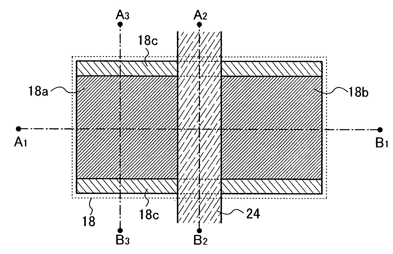
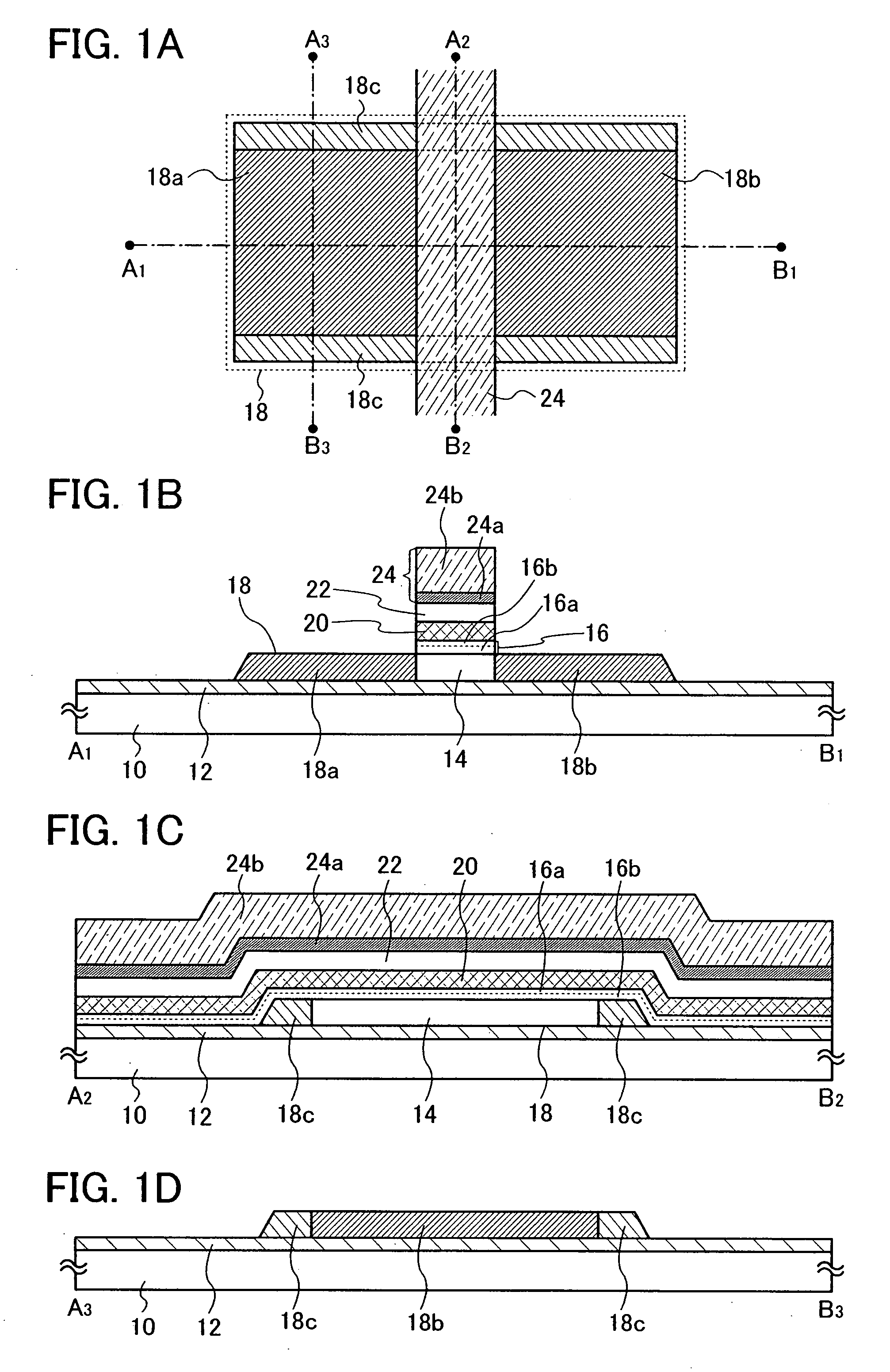
[0061]FIGS. 1A to 1D are views for explaining an example of a main structure of a nonvolatile semiconductor memory device of the present invention. FIGS. 1A to 1D each show a main part of a nonvolatile memory element provided in a memory portion, in the nonvolatile semiconductor memory device. It is to be noted that FIG. 1A shows a top view and FIGS. 1B, 1C, and 1D show schematic cross-sectional views taken along lines A1-B1, A2-B2, and A3-B3 of FIG. 1A, respectively.

[0062]The nonvolatile memory element shown in FIGS. 1A to 1D includes a substrate 10 having an insulating surface. As the substrate 10 having the insulating surface, the following can be used: a glass substrate, a quartz substrate, a sapphire substrate, a ceramic substrate, a metal substrate of which surface is provided with an insulating layer, or the like.

[006...

embodiment 1

[0116]In this embodiment, an example of a nonvolatile semiconductor memory device will be explained with reference to the drawings. It is to be noted that, in this embodiment, a case will be shown, where a nonvolatile memory element included in a memory portion and a transistor included in a logic portion for performing control or the like of the memory portion, which is provided over the same substrate as the memory portion are formed at the same time in the nonvolatile semiconductor memory device.

[0117]First, a view of a memory portion in the nonvolatile semiconductor memory device is shown in FIG. 8.

[0118]In the memory portion described in this embodiment, a plurality of memory cells each having a control transistor S and a nonvolatile memory element M is provided. In FIG. 8, one memory cell is formed by a control transistor S01 and a nonvolatile memory element M01. In a similar manner, a memory cell is formed by a control transistor S01 and a nonvolatile memory element M02; a me...
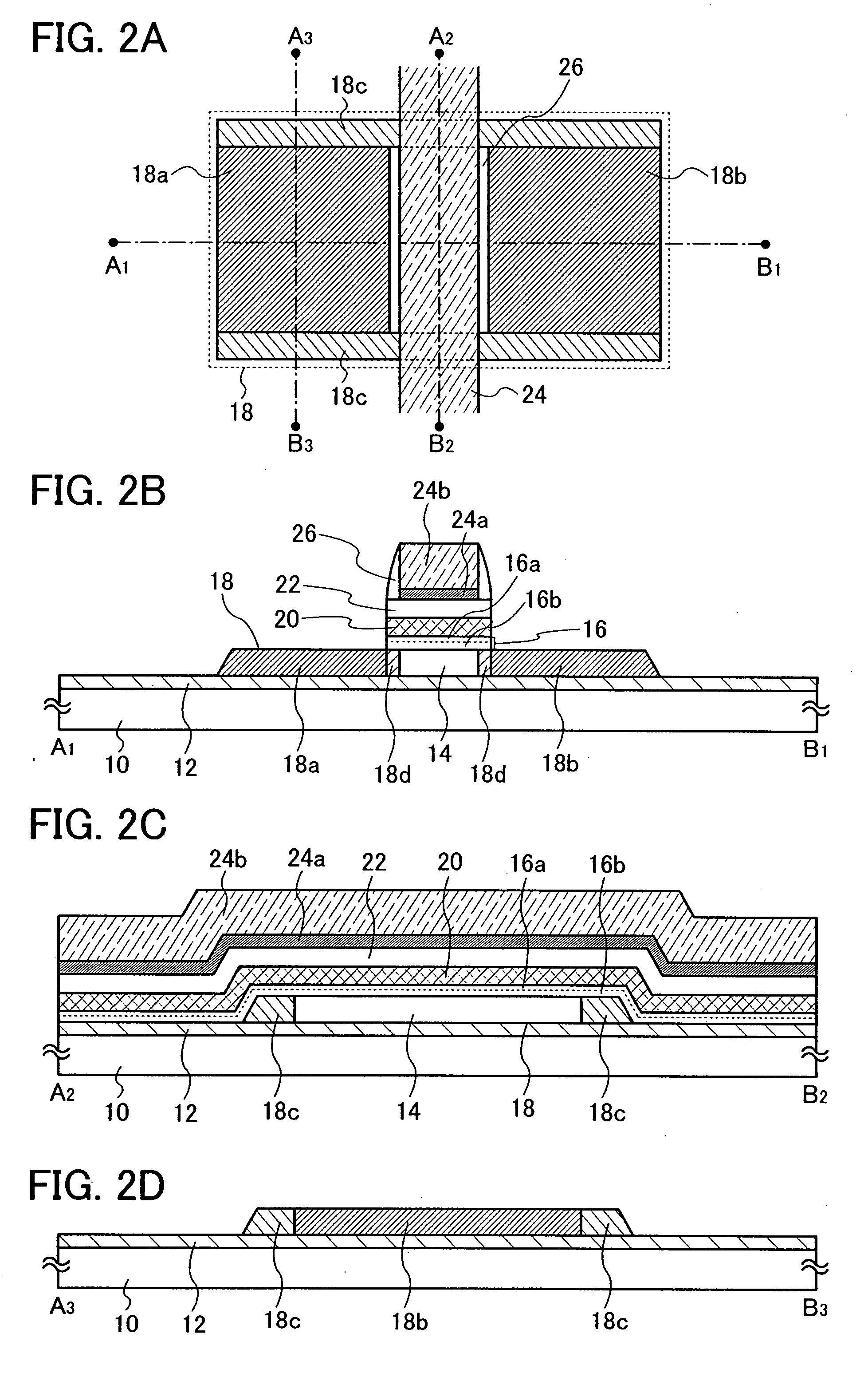
embodiment 2

[0169]In this embodiment, a manufacturing method of a nonvolatile semiconductor memory device that is different from the one explained in the above embodiment will be explained with reference to the drawings. It is to be noted that the same portions as those in the above embodiment are denoted by the same reference numerals and the explanation thereof is omitted. It is to be noted that, in FIGS. 29A to 29C, FIGS. 30A to 30C, and FIGS. 31A to 31C, portions taken along lines A-B and C-D show thin film transistors provided in logic portions, a portion taken along a line E-F shows a nonvolatile memory element provided in a memory portion, and a portion taken along a line G-H shows a thin film transistor provided in a memory portion.

[0170]First, as shown in the above embodiment, after a formation step similar to that shown in FIG. 19A, a resist 114 is selectively formed so as to cover an edge of each of semiconductor layers 104, 106, and 108, and a semiconductor layer 110, and then a fir...


PUM


Abstract

A nonvolatile semiconductor memory device is provided in such a manner that a semiconductor layer is formed over a substrate, a charge accumulating layer is formed over the semiconductor layer with a first insulating layer interposed therebetween, and a gate electrode is provided over the charge accumulating layer with a second insulating layer interposed therebetween. The semiconductor layer includes a channel formation region provided in a region overlapping with the gate electrode, a first impurity region for forming a source region or drain region, which is provided to be adjacent to the channel formation region, and a second impurity region provided to be adjacent to the channel formation region and the first impurity region. A conductivity type of the first impurity region is different from that of the second impurity region.

Description

BACKGROUND OF THE INVENTION[0001]1. Field of the Invention[0002]The present invention relates to a nonvolatile semiconductor memory device capable of electrical writing, reading, and erasing, and a manufacturing method thereof.[0003]2. Description of the Related Art[0004]In recent years, a market of a nonvolatile memory capable of electrically rewriting data and storing data even when power is turned off has been expanded. The nonvolatile memory has a similar structure to that of MOSFET (Metal Oxide Semiconductor Field Effect Transistor) and has a feature in that a region capable of accumulating charge for a long time is provided over a channel formation region. This charge accumulating region is formed over an insulating layer and is insulated and isolated from a peripheral region; accordingly, the charge accumulating region is also referred to as a floating gate. A control gate is provided over the floating gate with another insulating layer interposed therebetween.[0005]In a so-c...

Claims


Application Information

Patent Timeline
Patent Type & Authority Applications(United States)
IPC IPC(8): H01L27/10
CPCH01L21/84H01L27/115H01L27/12H01L27/11524H01L27/11521H10B41/35H10B69/00H10B41/30
Inventor TAKANO, TAMAEYAMAZAKI, SHUNPEI
Owner SEMICON ENERGY LAB CO LTD
Why Eureka
Try Eureka