Semiconductor device having device characteristics improved by straining surface of active region and its manufacture method

Inactive Publication Date: 2007-10-04
FUJITSU LTD
View PDF9 Cites 17 Cited by
  • Summary
  • Abstract
  • Description
  • Claims
  • Application Information

AI Technical Summary

Benefits of technology

[0029]It improves the device characteristics that the upper insulating film generates a tensile strain in the surface layer of the active region. Since the lower space of the trench is filled with the lower insulating film, an

Problems solved by technology

As a gate width becomes narrow, it is not possible to neglect strain caus

Method used


Image

  • Semiconductor device having device characteristics improved by straining surface of active region and its manufacture method
  • Semiconductor device having device characteristics improved by straining surface of active region and its manufacture method
  • Semiconductor device having device characteristics improved by straining surface of active region and its manufacture method

Examples


first embodiment

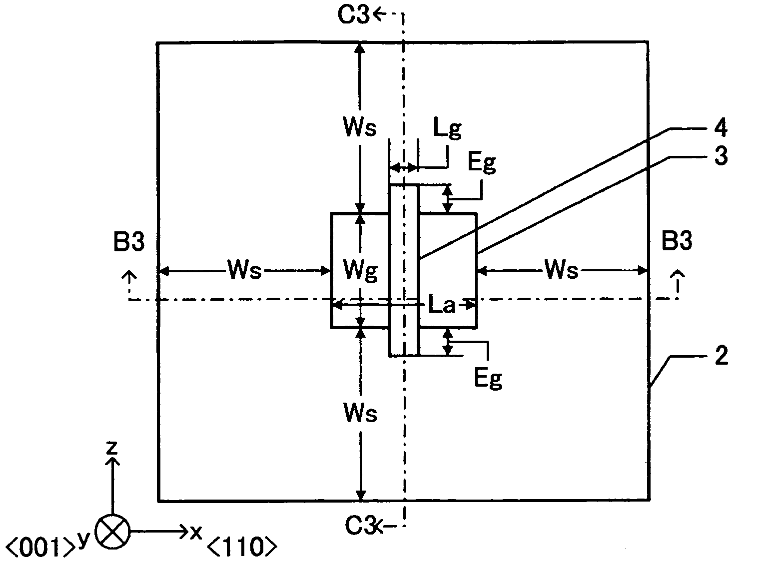
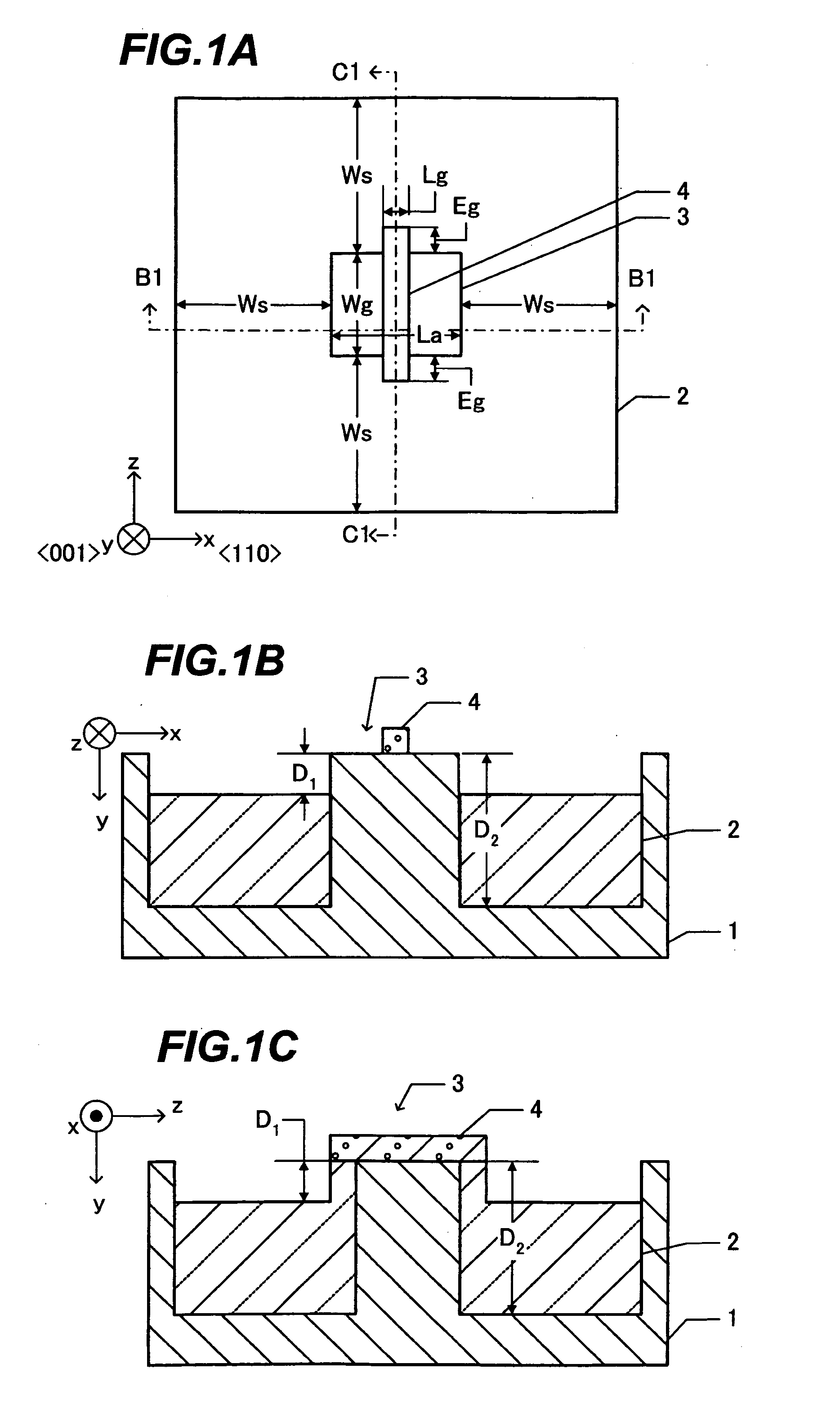
[0045]FIG. 3A is a plan view of a semiconductor device and FIGS. 3B and 3C are cross sectional views taken along one-dot chain lines B3-B3 and C3-C3 shown in FIG. 3A, respectively. The plan view shown in FIG. 3A is the same as the plan view shown in FIG. 1A, and the description thereof is omitted.

[0046]As shown in FIGS. 3B and 3C, a lower insulating film 22 fills a lower space of a trench formed in the surface layer of a semiconductor substrate 1 made of silicon. An upper insulating film 24 fills a space of the trench upper than the lower insulating film 22. The lower insulating film 22 and upper insulating film 24 constitute an isolation insulating film 2. The isolation insulating film 2 defines active region 3.

[0047]The upper surface of the isolation insulating film 2 sinks from the upper surface of the active region 3 by a depth D1. The upper surface of the upper insulating film 24 does not sink under the projected portions of a gate electrode 4 at opposite end portions thereof,...

second embodiment

[0064]Next, with reference to FIGS. 8A to 9B, description will be made on a semiconductor device manufacture method according to the

[0065]As shown in FIG. 8A, a principal surface of a semiconductor substrate 1 made of silicon is thermally oxidized to form a silicon oxide film 10. A thickness of the silicon oxide film 10 is set to 9 to 21 nm, for example, 10 nm. On the silicon oxide film 10, a silicon nitride film 11 is formed having a thickness of 100 to 150 nm, for example, 110 nm. The silicon nitride film 11 is formed by low pressure chemical vapor deposition (LPCVD) using mixture gas of SiCl2H2 and NH3 at a substrate temperature of 750° C. to 800° C.

[0066]As shown in FIG. 8B, an opening corresponding to an isolation insulating film to be formed is formed through the silicon nitride film 11 and silicon oxide film 10 by usual photolithography techniques. A width of the opening is 0.07 μm to 1 μm. Etching the silicon nitride film 11 and silicon oxide film 10 is performed by reactive...

third embodiment

[0096]Next, with reference to FIGS. 10A to 11B, description will be made on a semiconductor device manufacture method according to the

[0097]As shown in FIG. 10A, a lower insulating film 22 is formed by the same processes as those up to the state shown in FIG. 8F of the second embodiment. In the second embodiment, the upper insulating film 24 is deposited after the lower insulting film 22 is deposited. In the third embodiment, prior to depositing the upper insulating film 24, the substrate is immersed in HF aqueous solution having a density of 0.5% for 30 seconds to etch the surface layer of a lower insulating film 22.

[0098]As shown in FIG. 10B, this HF process thins a sidewall portion 22a of the lower insulating film 22 deposited on the inner surface of the trench 15. The subsequent processes are the same as those after the state of the second embodiment shown in FIG. 8G.

[0099]FIGS. 11A and 11B correspond to the cross sectional views taken along one-dot chain lines B3-B3 and C3-C3 s...


PUM


Abstract

A trench is formed in the surface layer of a semiconductor substrate, surrounding an active region. A lower insulating film made of insulating material fills a lower region of the trench. An upper insulating film fills a region of the trench above the lower insulating film. The upper insulating film has therein a stress generating tensile strain in a surface layer of the active region.

Description

CROSS REFERENCE TO RELATED APPLICATION[0001]This application is based on and claims priority of Japanese Patent Application No. 2006-094704 filed on Mar. 30, 2006, the entire contents of which are incorporated herein by reference.BACKGROUND OF THE INVENTION[0002]A) Field of the Invention[0003]The present invention relates to a semiconductor device and its manufacture method, and more particularly to a semiconductor device having device characteristics improved by straining the surface of an active region by an isolation insulating layer of a shallow trench isolation (STI) structure and its manufacture method.[0004]B) Description of the Related Art[0005]In a semiconductor device having an STI structure, the shallow trench is filled with an insulating film formed by chemical vapor deposition (CVD) using high density plasma. Thereafter, an unnecessary insulating film is removed by chemical mechanical polishing (CMP). Compressive strain exists in a silicon oxide film deposited by CVD us...

Claims


Application Information

Patent Timeline
IPC IPC(8): H01L29/76H01L21/336H01L21/76H01L29/78
CPCH01L21/76232H01L29/7846H01L29/045H01L29/6659H01L29/7833
Inventor KISHII, SADAHIROWATATANI, HIROFUMITERAHARA, MASANORITANABE, RYOSUZUKI, KAINASATOH, SHIGEO
Owner FUJITSU LTD
Why Eureka
Try Eureka