Nonvolatile semiconductor memory device and method for testing the same

a semiconductor memory and non-volatile technology, applied in semiconductor devices, digital storage, instruments, etc., can solve the problems of low erase efficiency, low erase efficiency during stress voltage application, and inability to test, so as to increase test coverage and device reliability

Inactive Publication Date: 2007-10-04
INFINEON TECH FLASH
View PDF4 Cites 16 Cited by
  • Summary
  • Abstract
  • Description
  • Claims
  • Application Information

AI Technical Summary

Benefits of technology

[0019] Test coverage and device reliability are increased as not only permanent (hard) short circuits but also near-short circuits are detectable. The device performance remains unaffected.

Problems solved by technology

For example with increasing number of erase cycles with high erase efficiency the erase efficiency may deteriorate.
The erase efficiency during application of the stress voltage is low and erase efficiency remains unaffected.

Method used


Image

  • Nonvolatile semiconductor memory device and method for testing the same
  • Nonvolatile semiconductor memory device and method for testing the same
  • Nonvolatile semiconductor memory device and method for testing the same

Examples


Embodiment Construction

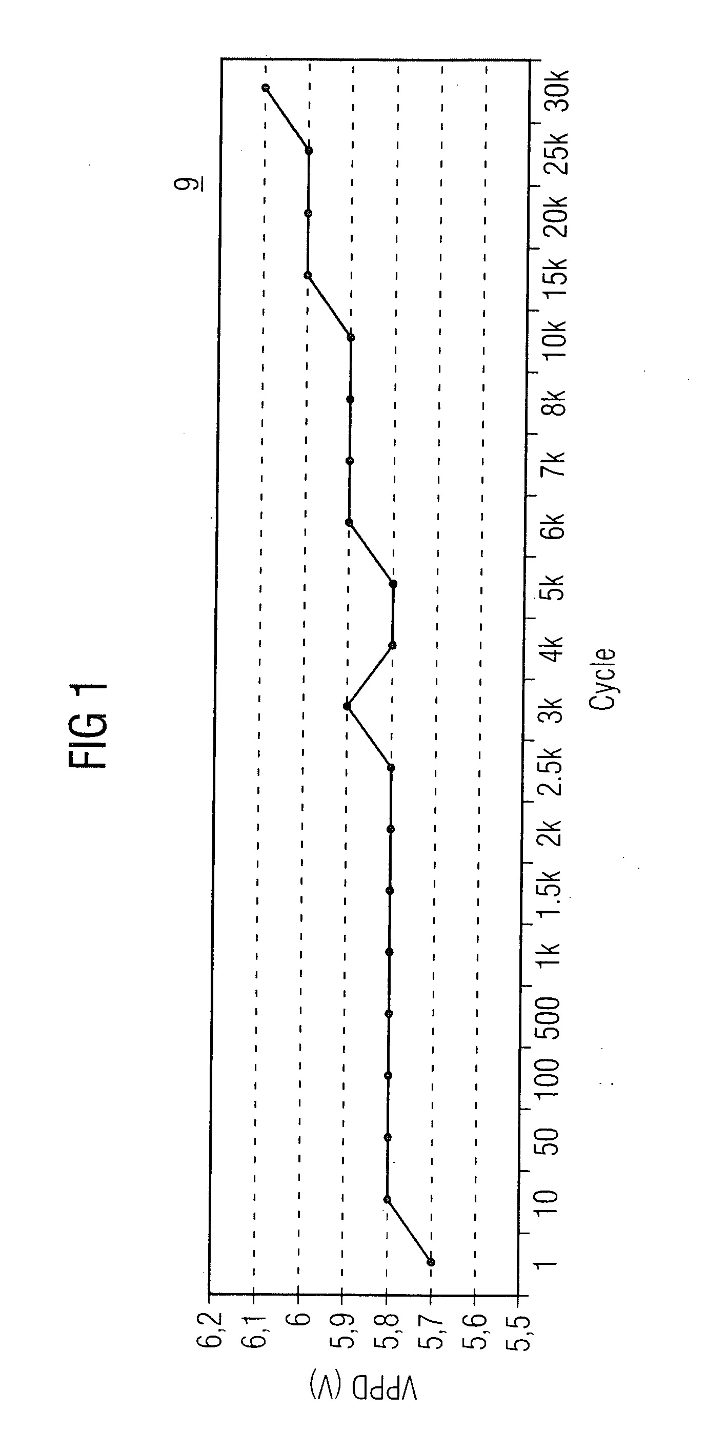
[0038]FIG. 1 illustrates a diagram 9 that plots the erase voltage, which is respectively required for reliably erasing an exemplary nonvolatile memory cell, against the number of erase cycles to which the exemplary nonvolatile memory cell has yet been subjected. The exemplary memory cell is a two-bit electrically erasable programmable read only memory device with a charge-trapping layer (NROM). Each of the NROM cell bits is programmed by channel hot electron injection and is erased by channel hot hole injection.

[0039] According to diagram 9, an erase voltage of 5.8 V is initially sufficient to reliably erase the exemplary memory cell during the first 1000 erase cycles. As the injection of the hot electrons in the charge trapping layer during programming and the injection of the hot holes being injected during erasing are not perfectly symmetrical, erase efficiency deteriorates significantly with increasing number of erase cycles. Therefore, with increasing number of erase cycles ha...


PUM


Abstract

A nonvolatile semiconductor memory device includes transistor-based memory cells. Each memory cell has a first and a second source/drain region, a channel region separating the first and the second source/drain region, a storage layer and a control gate. The control gates of the memory cells are connected to word lines. The first and second source/drain regions are connected to bit lines respectively. Each memory cell may be programmed by injecting first charge carriers of a first polarity and may be erased by injecting second charge carriers having the opposite polarity into the storage layer respectively. By applying a high stress voltage between bit line and word line, weak insulator structures may break through such that they become detectable as short-circuits by a low voltage leakage test. By applying the stress voltage contemporaneously on both sides of the memory cells, an early overerase/overprogram, resulting from hot carrier injection, is avoided.

Description

TECHNICAL FIELD [0001] The present invention relates to a nonvolatile electrically erasable programmable read only memory device, to a method of testing the nonvolatile electrically erasable programmable read only memory device and to a method of testing a memory cell of the nonvolatile electrically erasable programmable read only memory device. BACKGROUND OF INVENTION [0002] Nonvolatile electrically erasable programmable read only memory devices (EEPROMs), also known as nonvolatile semiconductor memory devices (NVM) comprise arrays of identical memory cells. Each memory cell bases on a MOSFET transistor including a source, a drain, an access or control gate, and a storing layer. [0003] The source and the drain are doped impurity diffusion regions being formed within a single crystalline semiconductor substrate and adjacent to a pattern surface of the semiconductor substrate. The doped impurity regions have a conductivity type that is opposite of that of the surrounding portion of t...

Claims


Application Information

Patent Timeline
Patent Type & Authority Applications(United States)
IPC IPC(8): G11C11/34G11C7/00G11C29/00G11C16/04
CPCG11C16/04G11C29/50G11C2029/5002H01L29/7923H01L27/115H01L27/11568H01L29/66833H01L21/28282H01L29/40117H10B43/30H10B69/00
Inventor HAUFE, JUERGSEIDEL, KONRAD
Owner INFINEON TECH FLASH
Why Eureka
Try Eureka