Method for fabricating semiconductor device having bulb-shaped recess gate

Inactive Publication Date: 2007-10-04
SK HYNIX INC
View PDF4 Cites 4 Cited by
  • Summary
  • Abstract
  • Description
  • Claims
  • Application Information

AI Technical Summary

Benefits of technology

[0010]In accordance with another aspect of the preset invention, a method for fabricating a semiconductor device is provided. A portion of a substrate is etched to form a recess having an upper portion and a lower portion. A polymer layer that fills the lower portion of the recess while exposing the upper portion of the recess is formed. A film is formed on sidewalls of the upper portion o

Problems solved by technology

A junction leakage is often generated due to an increased electric field.
Thus, it becomes difficult t

Method used


Image

  • Method for fabricating semiconductor device having bulb-shaped recess gate
  • Method for fabricating semiconductor device having bulb-shaped recess gate
  • Method for fabricating semiconductor device having bulb-shaped recess gate

Examples


Embodiment Construction

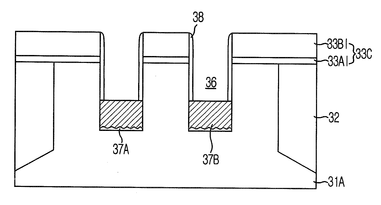
[0014]FIGS. 3A to 3F are cross-sectional views illustrating a method for fabricating a semiconductor device having bulb-shaped recess gates in accordance with an embodiment of the present invention. As shown in FIG. 3A, a shallow trench isolation (STI) process is performed on a substrate 31 to form an isolation structure 32. The isolation structure 32 defines an active region, and is formed at a depth that is greater than subsequent recesses (e.g., first recesses 36).

[0015]A hard mask layer 33 is formed over the substrate 31. The hard mask layer 33 is formed with a stack structure including a first hard mask layer 33A and a second hard mask layer 33B. The first hard mask layer 33A may include a dielectric-based hard mask layer, and the second hard mask layer 33B may include a silicon-based hard mask layer. Particularly, the first hard mask layer 33A is thinly formed using a dielectric material that may include a nitride layer or an oxide layer. The second hard mask layer 33B may inc...


PUM


Abstract

A method for fabricating a semiconductor device includes etching a portion of a substrate to form a recess. A polymer layer fills a lower portion of the recess. Sidewall spacers are formed over the recess above the lower portion of the recess. The polymer layer is removed. The lower portion of the recess is isotropically etching to form a bulb-shaped recess.

Description

CROSS-REFERENCE TO RELATED APPLICATIONS[0001]The present invention claims priority to Korean patent application number 10-2006-0029869, filed on Mar. 31, 2006 which is incorporated herein by reference in its entirety.BACKGROUND OF THE INVENTION[0002]The present invention relates to a method for fabricating a semiconductor device; and more particularly, to a method for fabricating a semiconductor device having a bulb-shaped recess gate.[0003]In a conventional method for forming a planar gate interconnection line, a gate is formed over a flat active region. The current demand for large scale integration of semiconductor devices has caused a decrease in channel length and an increase in implantation doping concentration. A junction leakage is often generated due to an increased electric field. Thus, it becomes difficult to secure a satisfactory refresh property of a device. Furthermore, a channel length and a channel width are restricted, and electron mobility is reduced due to the inc...

Claims


Application Information

Patent Timeline
IPC IPC(8): H01L21/465
CPCH01L29/4236H01L21/3083H01L21/18
Inventor CHO, JUN-HEE
Owner SK HYNIX INC
Why Eureka
Try Eureka