Manufacturing method for thin film transistor
a manufacturing method and transistor technology, applied in the direction of basic electric elements, electrical equipment, semiconductor devices, etc., can solve the problems of high volume and power consumption, and achieve the effects of reducing the number of manufacturing steps, improving the manufacturing yield of the array process, and reducing the cost of the manufacturing process
- Summary
- Abstract
- Description
- Claims
- Application Information
AI Technical Summary
Benefits of technology
Problems solved by technology
Method used
Image

Examples
Embodiment Construction
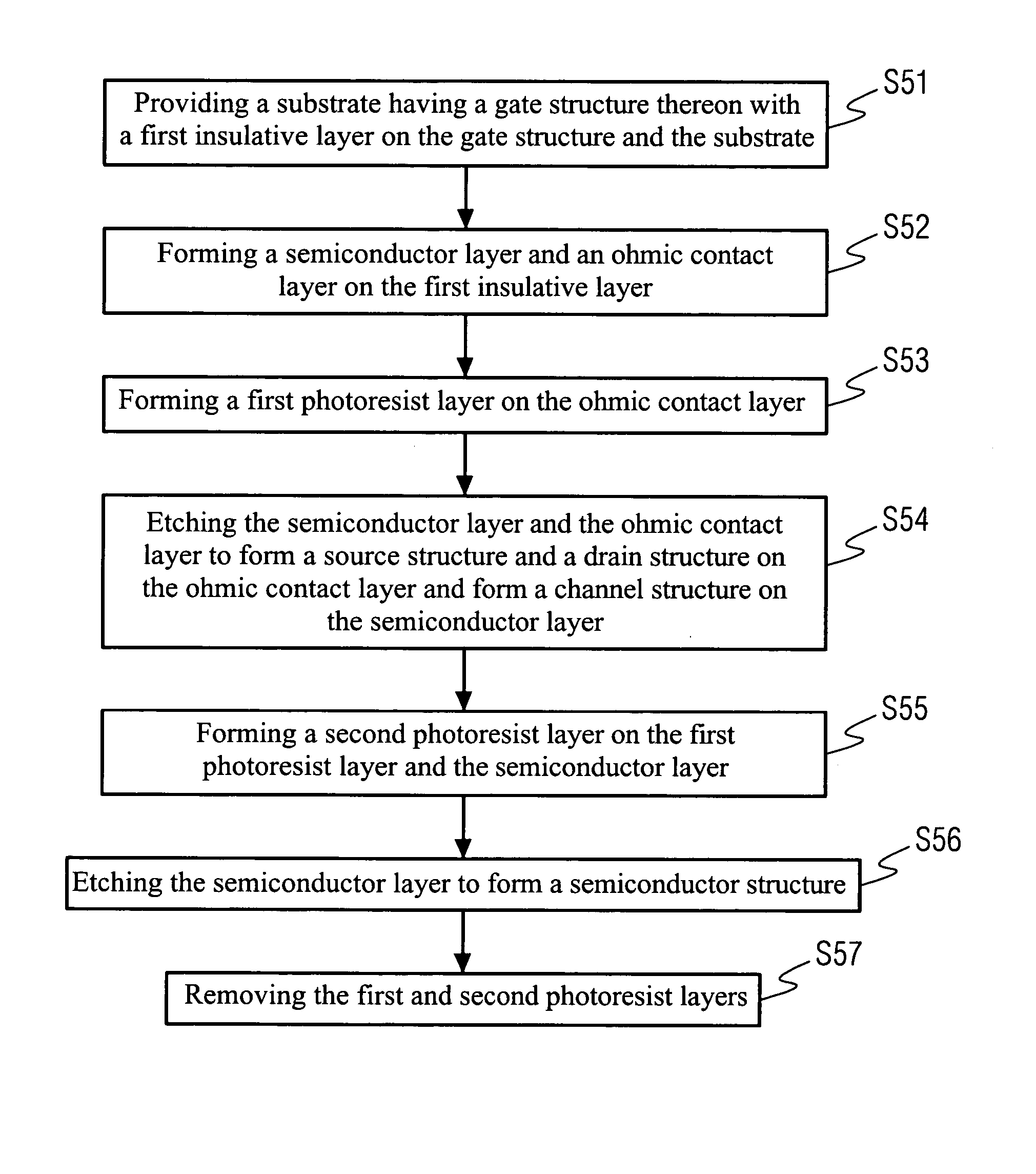
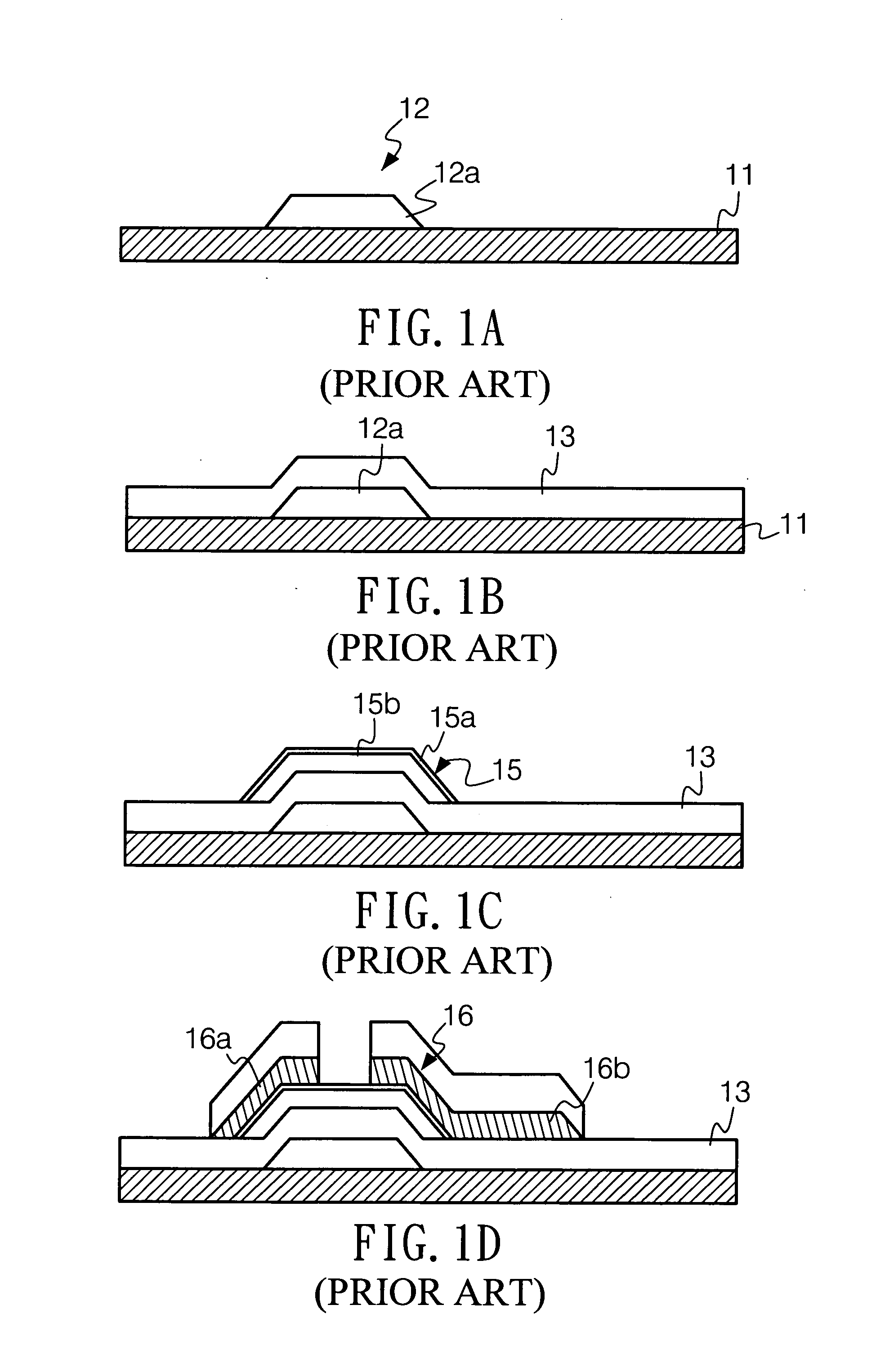
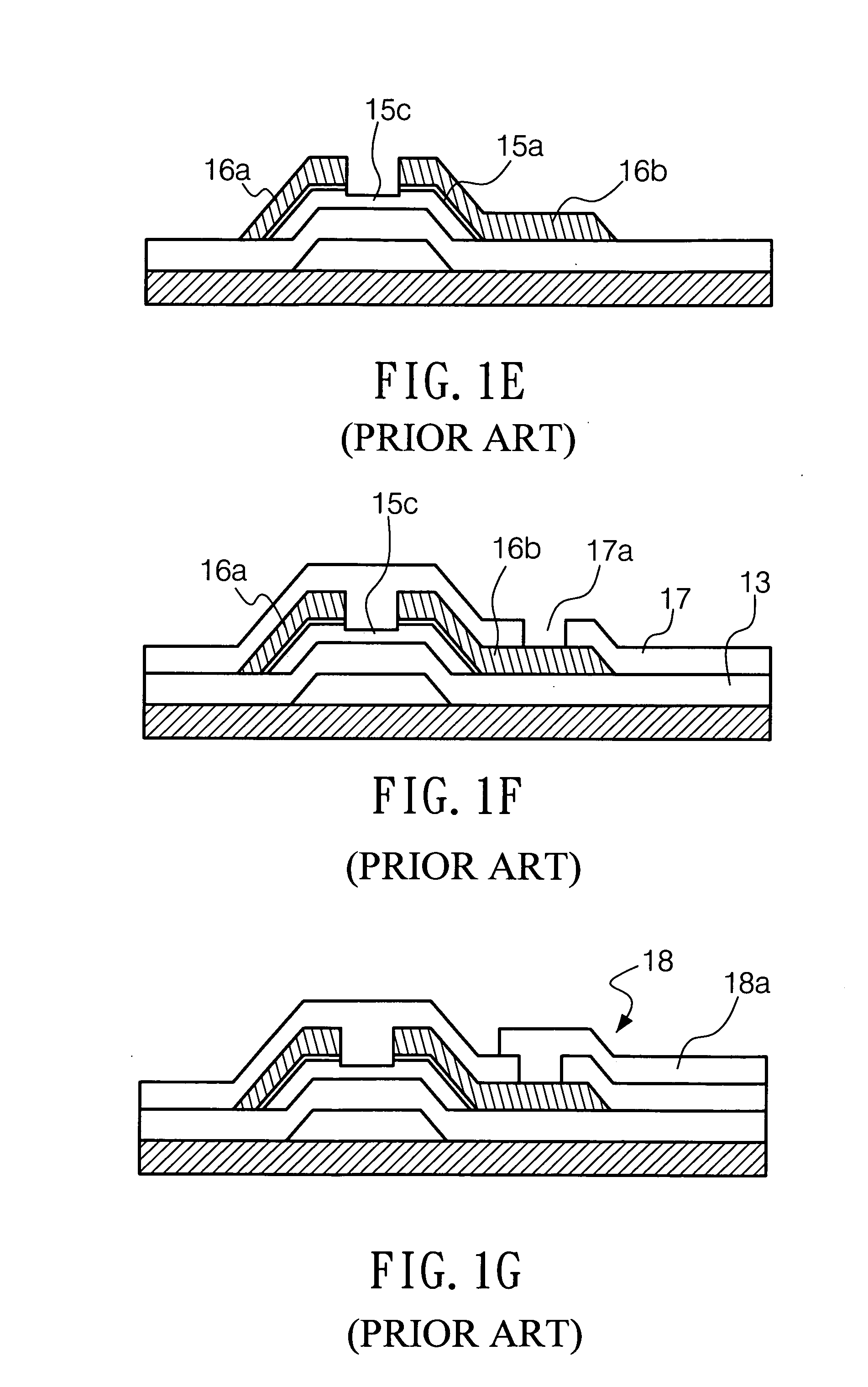
[0019]FIG. 3A to FIG. 3H show sectional views of a thin film transistor (TFT) structure after each manufacturing step is formed, respectively, according to the present invention. Referring first to FIG. 3A, a substrate 30 is first provided, which may be a glass substrate. Next, a metal layer 31 is formed on the substrate 30. The metal layer 31 may be formed of aluminum (Al), copper (Cu), wolfram (W), chromium (Cr) and other metals or a metallic alloy thereof by sputtering. Then, a gate structure 31a is defined on the metal layer 31 by using a first photomask (not shown) and subsequently formed through an etching process on the metal layer 31. Referring to FIG. 3B, a first insulative layer 32 and a semiconductor layer 33 are formed on the gate structure 31a and the substrate 30. The first insulative layer 32 may be made of silicon nitride (SiNx) and Silicon Oxide (SiOx) and the semiconductor layer 33 may be made of amorphous silicon (a-Si). Next, an ohmic contact layer 34 is formed o...
PUM
| Property | Measurement | Unit |
|---|---|---|
| semiconductor structure | aaaaa | aaaaa |
| semiconductor | aaaaa | aaaaa |
| transparent | aaaaa | aaaaa |
Abstract
Description
Claims
Application Information
 - Generate Ideas
- Intellectual Property
- Life Sciences
- Materials
- Tech Scout
- Unparalleled Data Quality
- Higher Quality Content
- 60% Fewer Hallucinations
Browse by: Latest US Patents, China's latest patents, Technical Efficacy Thesaurus, Application Domain, Technology Topic, Popular Technical Reports.
© 2025 PatSnap. All rights reserved.Legal|Privacy policy|Modern Slavery Act Transparency Statement|Sitemap|About US| Contact US: help@patsnap.com