[0056] Preparation of a COP plate with a concavo-convex grid shape transferred thereto.
[0057] Prepared was a
nickel stamper having on the surface a concavo-convex grid with the height of the concavo-convex grid of 230 nm. The concavo-convex grid was made by patterning using the
laser interference
exposure method, sinusoidal shape in cross section and streak grid shape in upper face. The dimensions of the plane were 500 mm both in length and width. Using the
nickel stamper, the concavo-convex grid shape was transferred to the surface of a cycloolefin resin (hereinafter, abbreviated as COP) plate with a thickness of 0.5 mm and length and width of 520 mm by
hot press method, and a COP plate with the concavo-convex grid shape transferred thereto was thus prepared. The
glass transition temperature (Tg) of the COP was 105° C.
[0058] More specifically,
hot press was performed as described below. First, a pressing
machine was evacuated, and the
nickel stamper and COP plate were heated to 190° C. After the nickel stamper and COP plate reached 190° C., the concavo-convex grid of the nickel stamper was transferred to the COP plate at a pressing pressure of 2 Mpa for four minutes of pressing time. Further, with the pressing pressure kept at 2 MPa, the nickel stamper and COP plate were cooled to 40° C., the vacuum was released, and then, the pressing pressure was released. When the pressing pressure was released, the nickel stamper and COP plate were easily removed. The
surface shape of the COP plate with the concavo-convex grid shape transferred thereto was observed using a field-emission
scanning electron microscope (hereinafter, abbreviated as FE-SEM) and it was confirmed that the concavo-convex grid shape of the nickel stamper was transferred faithfully.
[0060] Next, the COP plate with the concavo-convex grid shape transferred thereto was
cut into 520 mm×460 mm rectangles to be COP plates for drawing as drawing target members. At this point, the plates were
cut so that the longitudinal direction (520 mm) of the 520 mm×460 mm rectangle was substantially parallel with the longitudinal direction of the concavo-convex grid.
[0061]
Silicon oil was coated on surfaces of the COP plates for drawing by spray, and placed in a circular air oven at about 80° C. for 30 minutes. Next, the COP plate for drawing was fixed by chucks of a drawing
machine at its opposite ends of 10 mm in the longitudinal direction, and placed in this stat in a circular air oven with the temperature adjusted to 113÷1° C. for 10 minutes. Then, drawing was performed at speed of 250 mm / min, and finished when the distance between the chucks was drawn by five times, and twenty seconds later, the drawn COP plate was placed in an
atmosphere of
room temperature, and cooled with the distance between the chucks kept. The drawn COP plate was almost uniformly constricted at about 40% of the center portion, and the width of the most shrank portion was 200 mm. Similarly, the COP plates were drawn while changing only the distance between the chucks to 3.5 times and 2.5 times, and the minimum widths of the center portions of the drawn COP plates were 240 mm and 280 mm, respectively.
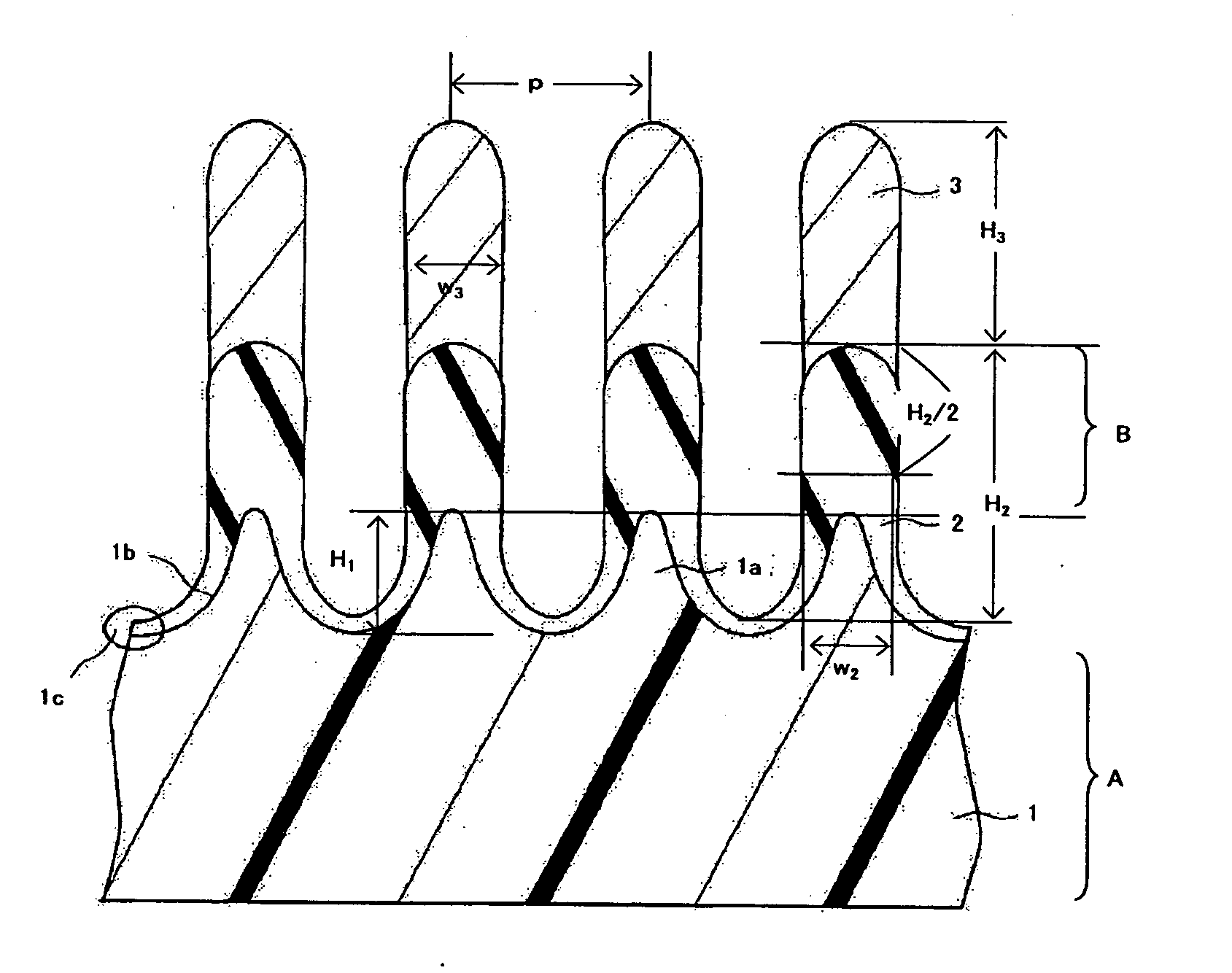
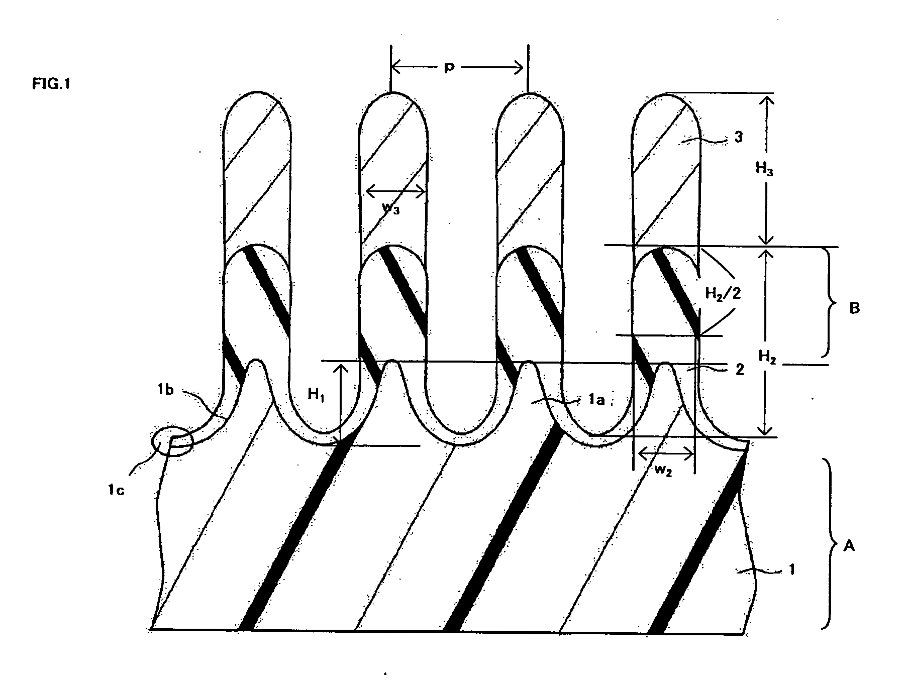
[0062] The surface and cross section of each of these three types of drawn COP plates were observed by FE-SEM, and it was understood that the
pitch and height of the microstructural concavo-convex grid of each of the plates were 100 nm / 95 nm (
pitch / height), 120 nm / 113 nm, or 140 nm / 133 nm, the cross section was in the sinusoidal shape, the shape from the upper face was a streak-shaped grid shape, and that the plates were shrank substantially in similar figures to the concavo-convex grid shape prior to the drawing.
