

Amorphous-carbon-based hard multilayer film and hard surface member having the film on surface
- Summary
- Abstract
- Description
- Claims
- Application Information
AI Technical Summary
Benefits of technology
Problems solved by technology
Method used
Image

Examples
example 1
[0045]Unbalanced magnetron sputtering apparatus having four evaporation sources (6 inches in target diameter) was used, and a target including each of elements M shown in the following Table 1 was mounted for two evaporation sources, and a carbon target was mounted for the remained, two evaporation sources. Mirror-polished substrates (cemented carbide (JIS-P20) substrate and high speed tool steel (JIS-SKH51, HRC63)) substrate were subjected to ultrasonic cleaning in ethanol, and then mounted on a turntable in a chamber of the sputtering apparatus. The chamber was evacuated (to a pressure of 1×10⁻³ Pa), and the substrates were heated to about 200° C. and then etched by Ar ions.
[0046]Next, a base layer, compositional gradient layer, and DLC layer as shown in the following Table 1 were formed in this order as follows.
1) Base Layer
[0047]A predetermined, atmospheric gas was introduced into the chamber, and each of the targets including the element M was supplied with electric power of 2 ...
example 2
[0074]A base layer, compositional gradient layer, and DLC layer as shown in the following Table 2 were formed and evaluated in the same way as in the example 1. A crystal structure of the base layer was examined by X-ray diffraction (CuKα line, 40 kV-40 mA) using the θ-2θ method, and a crystal structure corresponding to a peak having the highest intensity was determined as a crystal structure of the base layer.
[0075]Results are shown in Table 2. In the table, each sample in which a crystal structure of the base layer is made to be the α-W structure, α-Mo structure or TaN structure exhibits intensity of a maximum peak of the α-W structure, α-Mo structure, or TaN structure, showing at least five times as large as intensity of peaks of other crystal structures.
TABLE 2CompositionAdhesionBase LayerChange LayerDLC layer(Critical Load (N))Element MCompositionThicknessCrystalThicknessCompositionThicknessSintered HardHigh Speed ToolNo.(Target)(Atomic Ratio)(nm)StructureType*(nm)(Atomic Ratio...
example 3
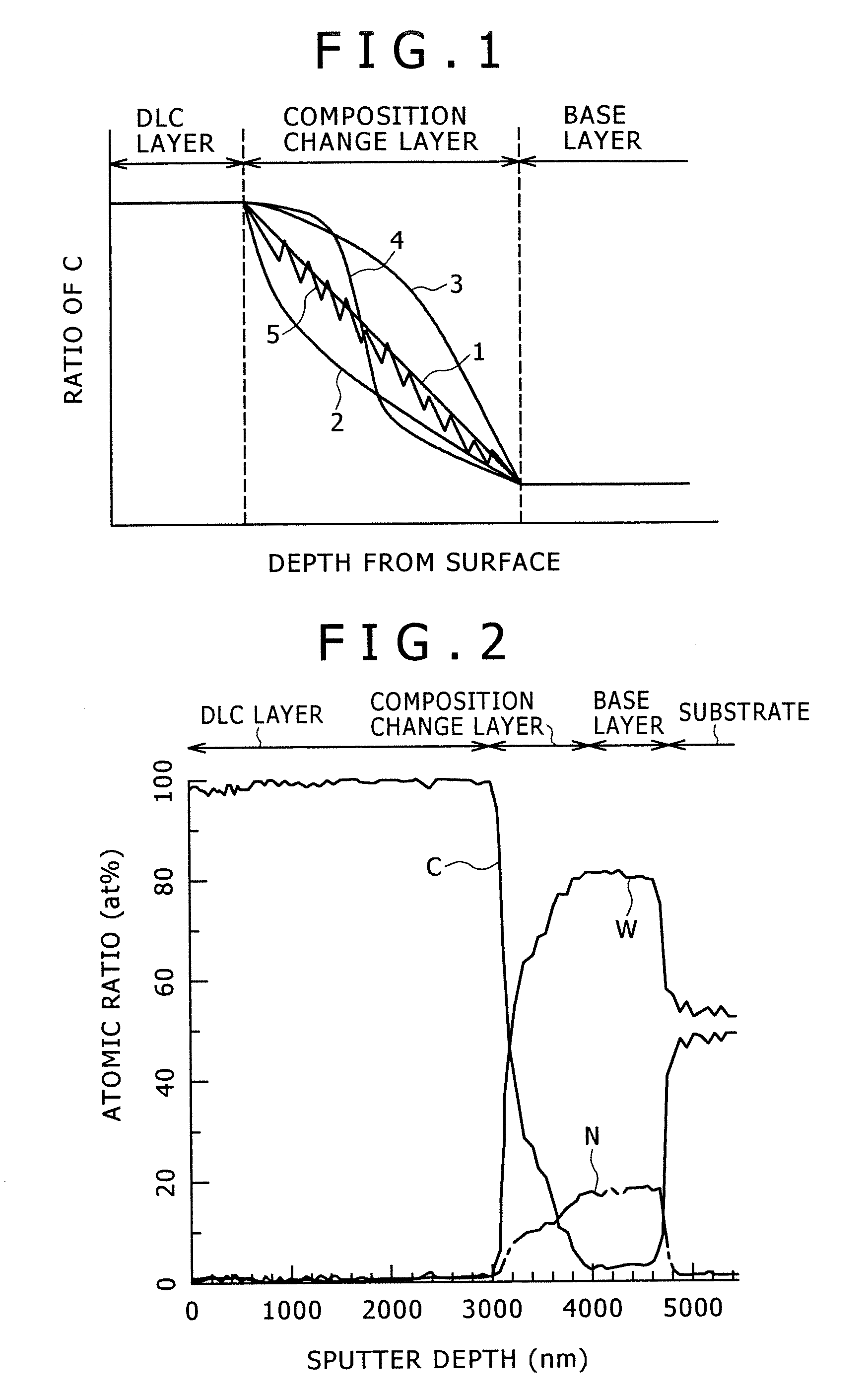
[0078]A base layer, compositional gradient layer, and DLC layer as shown in the following Table 3 were formed and evaluated in the same way as in the example 1. In samples of Nos. 19 to 23, a composition change pattern of the compositional gradient layer was variously changed as shown in FIG. 1.
TABLE 3CompositionBase LayerChange LayerDLC LayerAdhesionElement MCompositionThicknessThicknessCompositionThickness(Critical Load (N))No.(Target)(Atomic Ratio)(nm)Type*(nm)(Atomic Ratio)(μm)Sintered Hard AlloyHigh Speed Tool Alloy1WW0.8N0.21001500C2100 or more902WW0.7C0.1N0.21001500C2100 or more853WW0.5C0.3N0.21001500C280754WW0.4C0.5N0.11001500C280705WW0.4C0.61001500C270606MoMo0.85N0.1501500C250457MoMo0.85N0.1551500C270658MoMo0.85N0.15101500C295859MoMo0.85N0.151001500C2100 or more8510MoMo0.85N0.152001500C2100 or more8511MoMo0.85N0.1520001500C2100 or more8012MoMo0.85N0.151000001500C2100 or more8013WW0.8N0.210010C2504014WW0.8N0.210015C2908515WW0.8N0.2100120C2958516WW0.8N0.21001100C2100 or more9...
PUM
| Property | Measurement | Unit |
|---|---|---|
| Percent by atom | aaaaa | aaaaa |
| Current | aaaaa | aaaaa |
| Current | aaaaa | aaaaa |
Abstract
Description
Claims
Application Information