Semiconductor integrated circuit system, semiconductor integrated circuit, operating system, and control method for semiconductor integrated circuit

a technology of integrated circuits and semiconductors, applied in the field can solve problems such as unnecessary giving an excessive margin in circuit design, and achieve the effect of improving the performance of semiconductor integrated circuits

Active Publication Date: 2007-11-01
PANASONIC SEMICON SOLUTIONS CO LTD
View PDF10 Cites 12 Cited by
  • Summary
  • Abstract
  • Description
  • Claims
  • Application Information

AI Technical Summary

Benefits of technology

[0020]Since the present invention allows adaptive correction control and the removal of an excessive margin, the performance of the semiconductor integrated circuit can be improved.

Problems solved by technology

The arrangement constantly holds the operation of the program normal so that it is unnecessary to give an excessive margin in designing the circuit.

Method used


Image

  • Semiconductor integrated circuit system, semiconductor integrated circuit, operating system, and control method for semiconductor integrated circuit
  • Semiconductor integrated circuit system, semiconductor integrated circuit, operating system, and control method for semiconductor integrated circuit
  • Semiconductor integrated circuit system, semiconductor integrated circuit, operating system, and control method for semiconductor integrated circuit

Examples


Embodiment Construction

[0045]Referring to the drawings, an embodiment of the present invention will be described herein below.

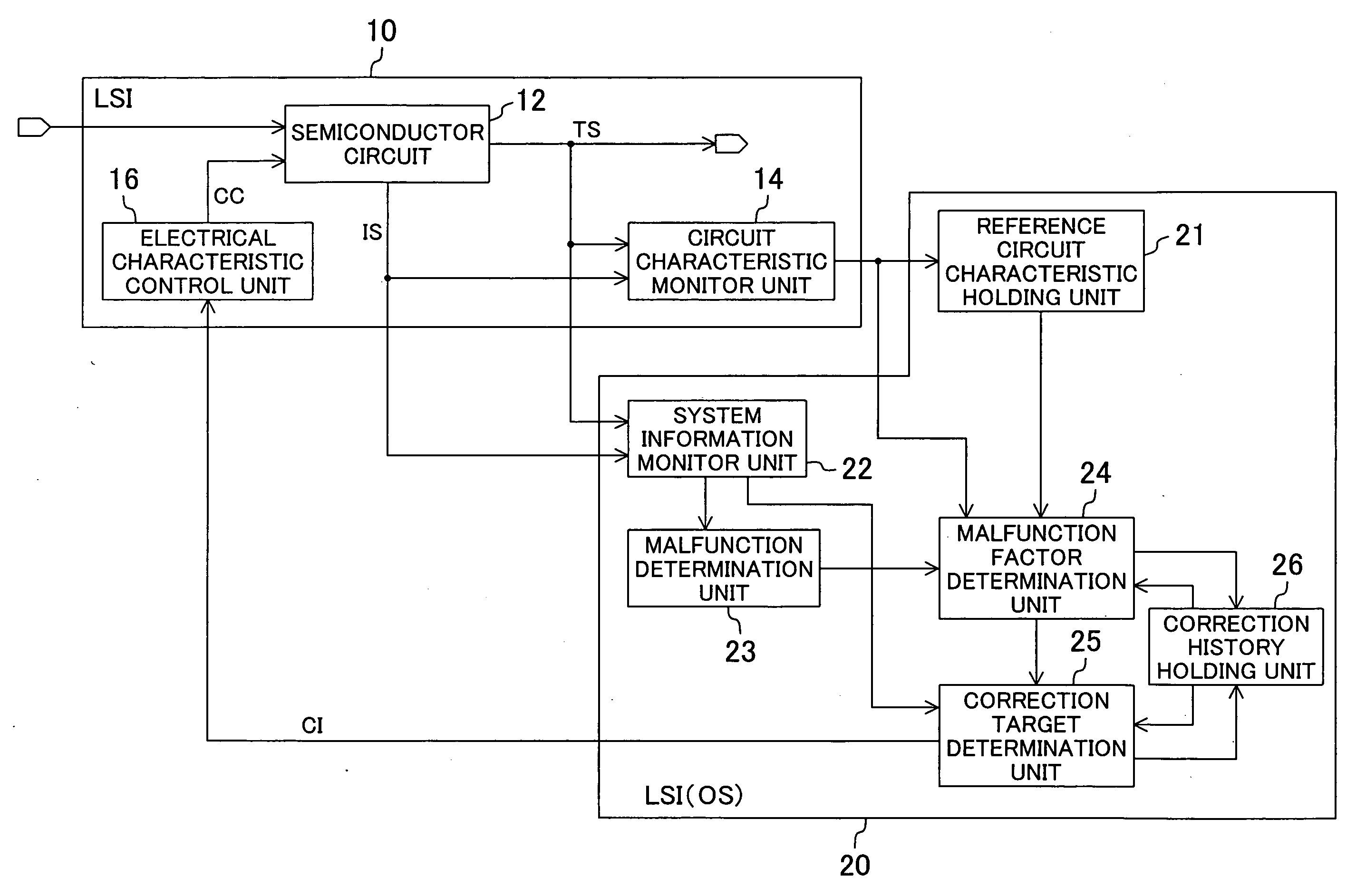
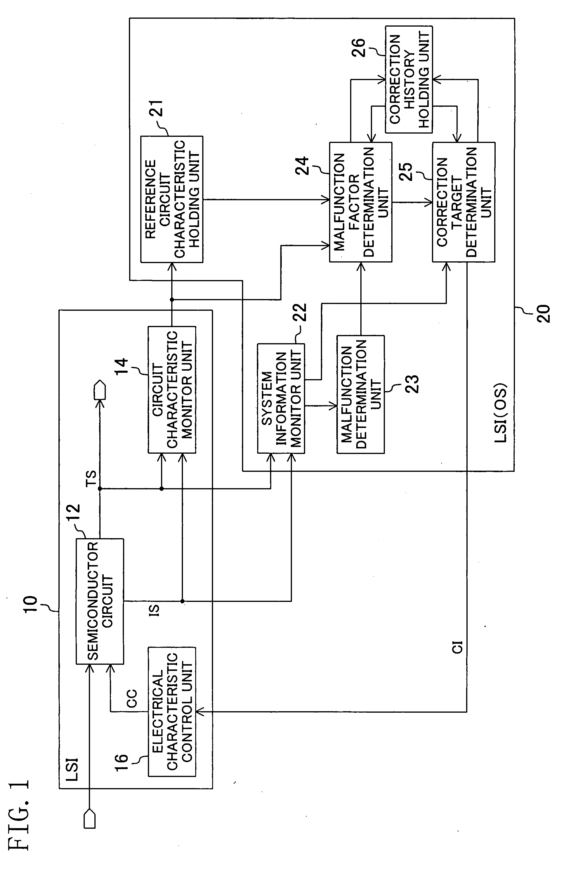
[0046]FIG. 1 is a block diagram showing a structure of a semiconductor integrated circuit system according to the embodiment of the present invention. The system of FIG. 1 comprises semiconductor integrated circuits (LSIs) 10 and 20. The LSI 10 has a semiconductor circuit 12 as a control target circuit, a circuit characteristic monitor unit 14, and an electrical characteristic control unit 16. The LSI 20 comprises a reference circuit characteristic holding unit 21, a system information monitor unit 22, a malfunction determination unit 23, a malfunction factor determination unit 24, a correction target determination unit 25, and a correction history holding unit 26.

[0047]The LSIs 10 and 20 may be constructed as different chips or as a single chip. The LSI 20 implements the function of each of the components by means of an operating system (OS) executed on the circuit hereof. The OS ...


PUM


Abstract

A semiconductor integrated circuit system has a control target circuit executing a program, a system information monitor unit for outputting system information indicating a state of the control target circuit, a circuit characteristic monitor unit for determining a circuit characteristic of the control target circuit and outputting the circuit characteristic as circuit characteristic information, a malfunction determination unit for determining whether or not the control target circuit is normally operating based on the system information, a reference circuit characteristic holding unit for holding the circuit characteristic information as reference circuit characteristic information when the control target circuit is normally operating, a malfunction factor determination unit for determining a malfunction factor based on the circuit characteristic information and on the reference circuit characteristic information when the control target circuit is not normally operating, and a correction target determination unit for determining a correction target in the control target circuit.

Description

CROSS REFERENCE TO RELATED APPLICATIONS[0001]The teachings of Japanese Patent Applications JP 2006-114814, filed Apr. 18, 2006, and JP 2007-57388, filed Mar. 7, 2007, are entirely incorporated herein by reference, inclusive of the claims, specifications, and drawings.BACKGROUND OF THE INVENTION[0002]The present invention relates to a semiconductor integrated circuit and, more particularly, to a technology for preventing the malfunction of a semiconductor integrated circuit resulting from a change in the electrical characteristics thereof.[0003]In designing a semiconductor integrated circuit, a so-called signal integrity (SI) verification is performed which verifies and guarantees that a malfunction due to noise does not occur by performing simulation (see Japanese Laid-Open Patent Publication No. 9-305649). On the other hand, a noise margin improvement method based on the control of a substrate voltage has been proposed. In this case, to implement a constant threshold voltage or sat...

Claims


Application Information

Patent Timeline
Patent Type & Authority Applications(United States)
IPC IPC(8): G06F11/00G01R31/28
CPCG01R31/31708
Inventor SASAGAWA, YUKIHIRO
Owner PANASONIC SEMICON SOLUTIONS CO LTD
Why Eureka
Try Eureka