Process for producing a iii-n bulk crystal and a free-standing iii-n substrate, and iii-n bulk crystal and free-standing iii-n substrate

a technology of iiin bulk crystal and free-standing iiin substrate, which is applied in the direction of crystal growth process, electrical apparatus, basic electric elements, etc., can solve the problems of long production process time, insufficient quality of substrates, and inability to meet the requirements of production, and achieve excellent crystal quality.

Active Publication Date: 2007-11-08
FREIBERGER COMPOUND MATERIALS
View PDF8 Cites 37 Cited by
  • Summary
  • Abstract
  • Description
  • Claims
  • Application Information

AI Technical Summary

Benefits of technology

[0007] An object of the present invention is to provide a process for producing III-N bulk crystals, and to provide III-N substrates, respectively having excellent crystal quality and a homogenous distribution thereof in the direction of growth and / or in the plane being perpendicular thereto.
[0010] According to a second aspect, the present invention provides a process for preparing a III-N bulk crystal, wherein III denotes at least one element from group III of the periodic system, selected from Al, Ga and In, wherein the III-N bulk crystal, is grown on a substrate or a template by means of vapor phase epitaxy, and wherein the growth rate is maintained essentially constant at least one value during epitaxial growth. The process operation according to the invention enables essentially maintaining the growth rate during a main part, preferably during essentially the whole process and, if desired, during the complete process for the growth of the bulk crystal to the desired length. The term “essentially constant” used according to the invention means that the inventive crystal quality described in further detail below can be achieved. In a preferred embodiment, a correction or adjustment to an actually constant growth rate is carried out, when the method for measuring the growth rate determines a difference of maximally 10%, particularly a difference of maximally 5%, and above all a difference of maximally 2% when comparing the actual growth rate with the nominal (desired) growth rate. In a further preferred manner, the growth rate is exactly constant, i.e. lying within the control accuracy (standard deviation ±0.5%). During the whole growth process for the III-N bulk crystal of desired thickness, the growth rate can be maintained at one predetermined value; or the growth rate may be maintained, in partial periods, at multiple different predetermined, yet respectively constant values.
[0025] After carrying out the process according to the invention, free-standing III-N crystal substrates can be easily produced by separating one or more III-N substrates from the III-N bulk crystal. Various suitable methods for separation are known, wire sawing being a particularly suitable one. Subsequently, further treatment steps can be carried out, where lapping, polishing (chemical, and / or mechanical), etching (wet and / or dry), subsequent thermal treatment, conditioning in gas atmosphere (suitably containing at least ammonia), and / or any desirable finishing or cleaning steps can be particularly exemplified.

Problems solved by technology

Until now, however, such substrates have not been available in sufficient quality.
This is largely caused by difficulties in conventional bulk growth technologies due to the extremely high steady state vapor pressure of nitrogen over III-N compounds at typical growth temperatures.
This process provides qualitatively valuable GaN bulk material, but has the disadvantage that, up to now, only small GaN substrates with a surface area of maximally 100 mm2 can be produced thereby.
Furthermore, the production process requires a long production time in comparison with other processes and is technologically laborious and cost-intensive due to the extremely high growth pressures.
Drawbacks of the aforementioned methods lie on the one hand in the relatively high costs due to the complex technologies for substrate separation, and on the other hand in the fundamental difficulty to produce III-N materials having a homogenously low defect density.

Method used


Image

  • Process for producing a iii-n bulk crystal and a free-standing iii-n substrate, and iii-n bulk crystal and free-standing iii-n substrate
  • Process for producing a iii-n bulk crystal and a free-standing iii-n substrate, and iii-n bulk crystal and free-standing iii-n substrate
  • Process for producing a iii-n bulk crystal and a free-standing iii-n substrate, and iii-n bulk crystal and free-standing iii-n substrate

Examples


examples

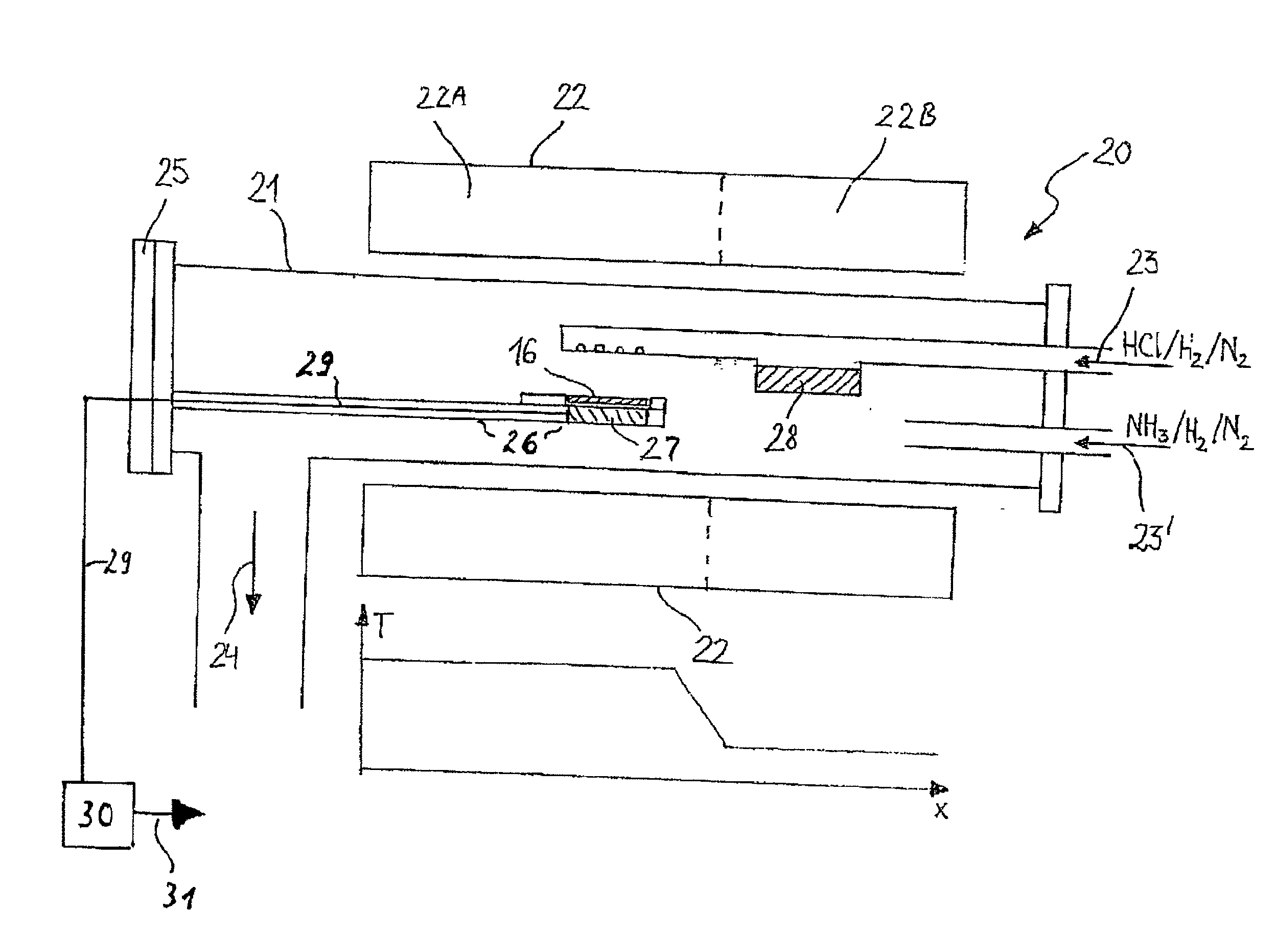
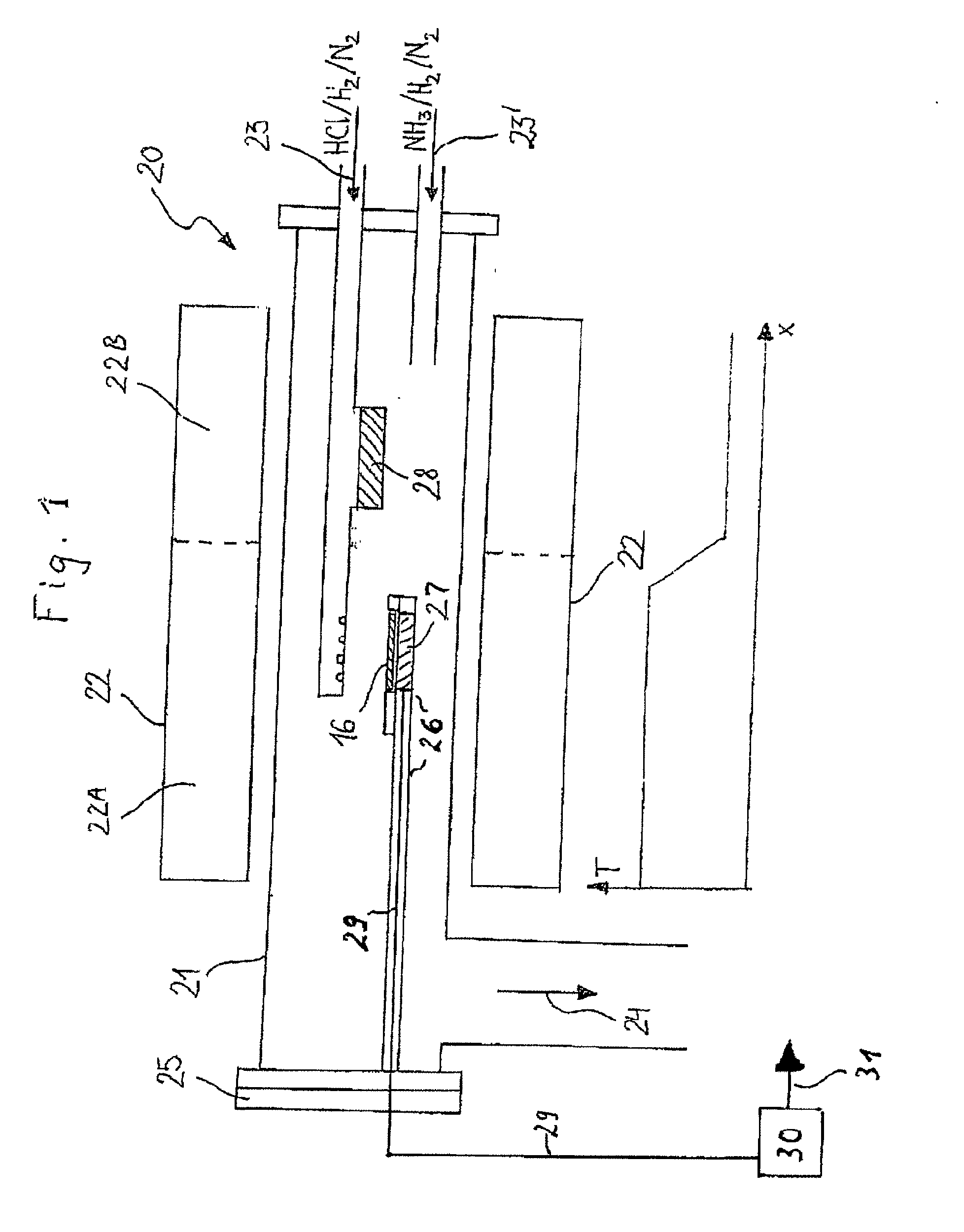
[0082] A GaN substrate having a diameter of 50 to 60 mm is loaded into an Aixtron LP-HVPE reactor. The reactor is modified such that the weight of the growing GaN bulk crystal can be determined in real-time by means of a weighing module or load cell which measures the weight of the crystal including substrate holder and susceptor. The load cell, which is based on the geometry of a platform weighing module with beam bending and force feedback, is a load cell of type S2 of the company Hottinger Baldwin Meβtechnik GmbH (Darmstadt, Germany). The output signal is processed by a measurement amplifier. A bulk GaN crystal having a thickness of several mm is grown on the substrate. For example, the HVPE process takes place at a temperature of 1,040° C. to 1,075° C. and a pressure of 900 to 1,000 mbar with a V / III ratio of about 50 and a carrier gas composition of about 50% hydrogen and 50% nitrogen. The growth rate is 220 μm / h and is measured in real-time, and is and controlled in situ by ad...


PUM

PropertyMeasurementUnit
diameteraaaaaaaaaa
lengthaaaaaaaaaa
lengthaaaaaaaaaa

Abstract

Embodiments of the invention relate to a process for producing a III-N bulk crystal, wherein III denotes at least one element selected from group III of the periodic system, selected from Al, Ga and In, wherein the III-N bulk crystal is grown by vapor phase epitaxy on a substrate, and wherein the growth rate is measured in real-time. By actively measuring and controlling the growth rate in situ, i.e. during the epitaxial growth, the actual growth rate can be maintained essentially constant. In this manner, III-N bulk crystals and individualized III-N single crystal substrates separated therefrom, which respectively have excellent crystal quality both in the growth direction and in the growth plane perpendicular thereto, can be obtained.

Description

CROSS-REFERENCE TO RELATED PATENT APPLICATIONS [0001] This application claims priority from U.S. Provisional Application 60 / 798,314, filed May 8, 2006, incorporated herein by reference in its entirety.BACKGROUND OF THE INVENTION [0002] The present invention relates to processes for producing III-N bulk crystals from a gas or vapor phase, an well as to a process for producing free-standing III-N substrates which are obtained from the III-N bulk crystals. The term “III-N” denotes a III-N compound, where III denotes at least one element of group III of the periodic table of elements, selected from aluminum, gallium and indium (in the following sometimes abbreviated by (Al, Ga, In)), and N denotes nitrogen. The III-N bulk crystal and the free-standing III-N substrate comprise the III-N compound as the main material, and they are respectively preferably composed essentially of or completely of the III-N compound, optionally together with impurities. The invention further relates to III-N...

Claims


Application Information

Patent Timeline
Patent Type & Authority Applications(United States)
IPC IPC(8): H01L29/20C30B29/38
CPCC30B25/00C30B25/16Y10T117/1004C30B29/403Y10T117/1008C30B29/40
Inventor LEIBIGER, GUNNARHABEL, FRANKEICHLER, STEFAN
Owner FREIBERGER COMPOUND MATERIALS
Why Eureka
Try Eureka