Fabrication of vertical sidewalls on (110) silicon substrates for use in si/sige photodetectors

a technology of silicon substrate and silicon substrate, applied in the field of near-infrared photodetectors, can solve the problems of small critical thickness, high dark current, and inevitable lattice defects in sige, and achieve the effect of improving the quantum efficiency of photodetectors

Active Publication Date: 2007-11-08
SHARP KK AKA SHARP CORP +1
View PDF5 Cites 190 Cited by
  • Summary
  • Abstract
  • Description
  • Claims
  • Application Information

AI Technical Summary

Benefits of technology

[0012] It is an object of the invention to improve the quantum efficiency of photodetectors, e.g., near-IR photodetectors, integrated on silicon substrates.

Problems solved by technology

A high germanium concentration and high device process temperature result in a smaller critical thickness.
Once the SiGe thickness is grown above its critical thickness, lattice defects in SiGe are inevitable.
An IR photo detector built on SiGe containing lattice defects will have a high dark current and produce electronic noise.
However, this does not allow the device to be used in image detection.
However, referring to FIG. 2, reactive ion-etching (RIE) of silicon usually results in a sloped sidewall, shown generally at 10, and in poor crystal quality near the sidewall surface, as shown generally at 12, where a damaged area of silicon is formed near an RIE-etched sidewall.
Also, the surface is often rather rough.
However, such an etch process is not known in the prior art.
In addition, the use of a selective wet etch instead of RIE results in undamaged crystalline silicon at the sidewall surfaces.

Method used


Image

  • Fabrication of vertical sidewalls on (110) silicon substrates for use in si/sige photodetectors
  • Fabrication of vertical sidewalls on (110) silicon substrates for use in si/sige photodetectors
  • Fabrication of vertical sidewalls on (110) silicon substrates for use in si/sige photodetectors

Examples


Embodiment Construction

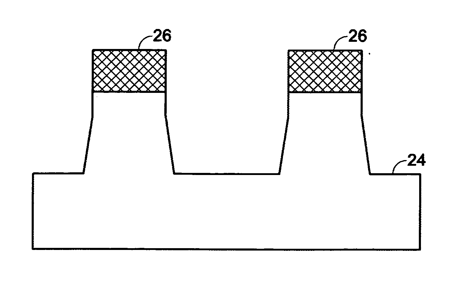
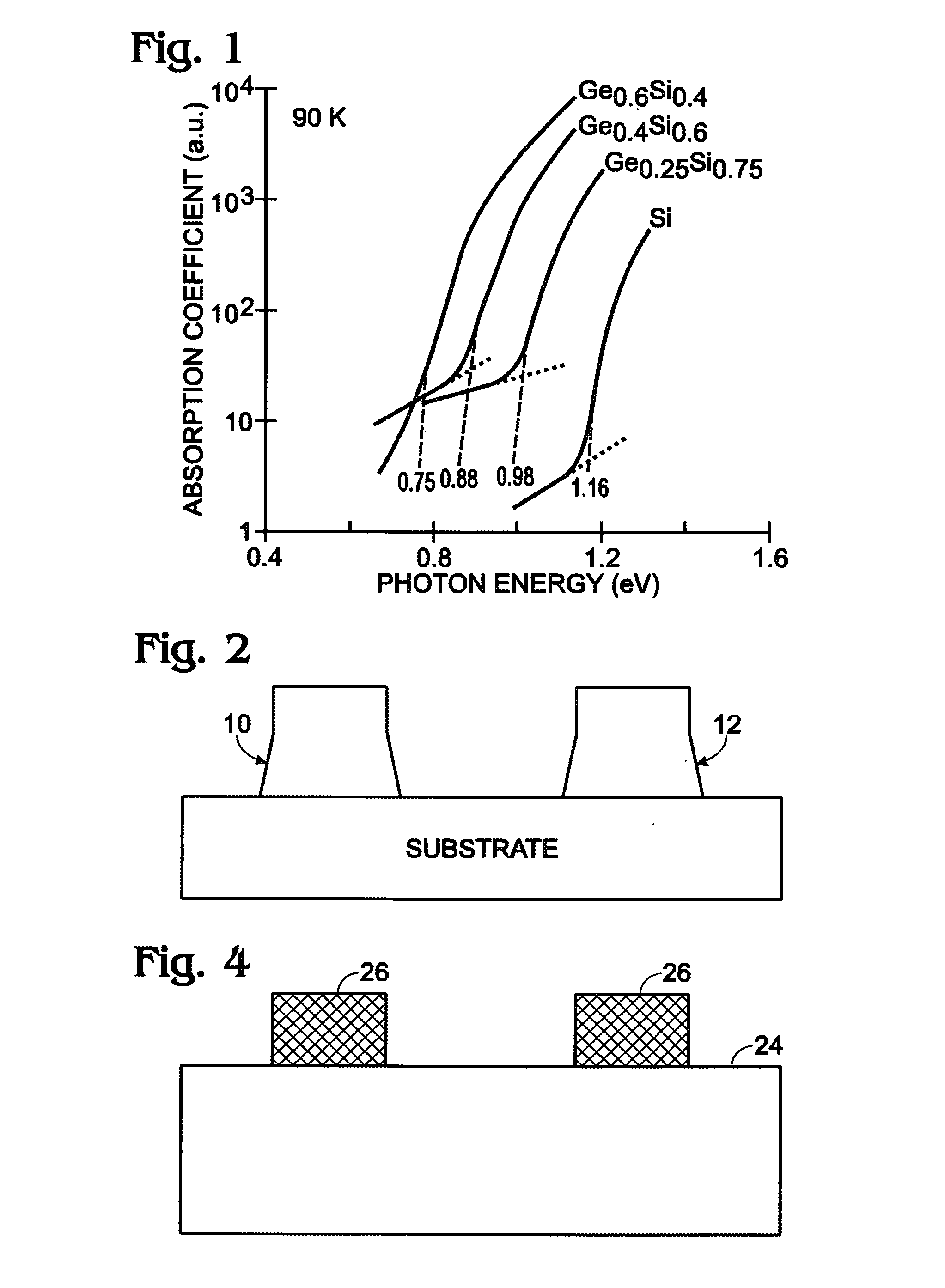
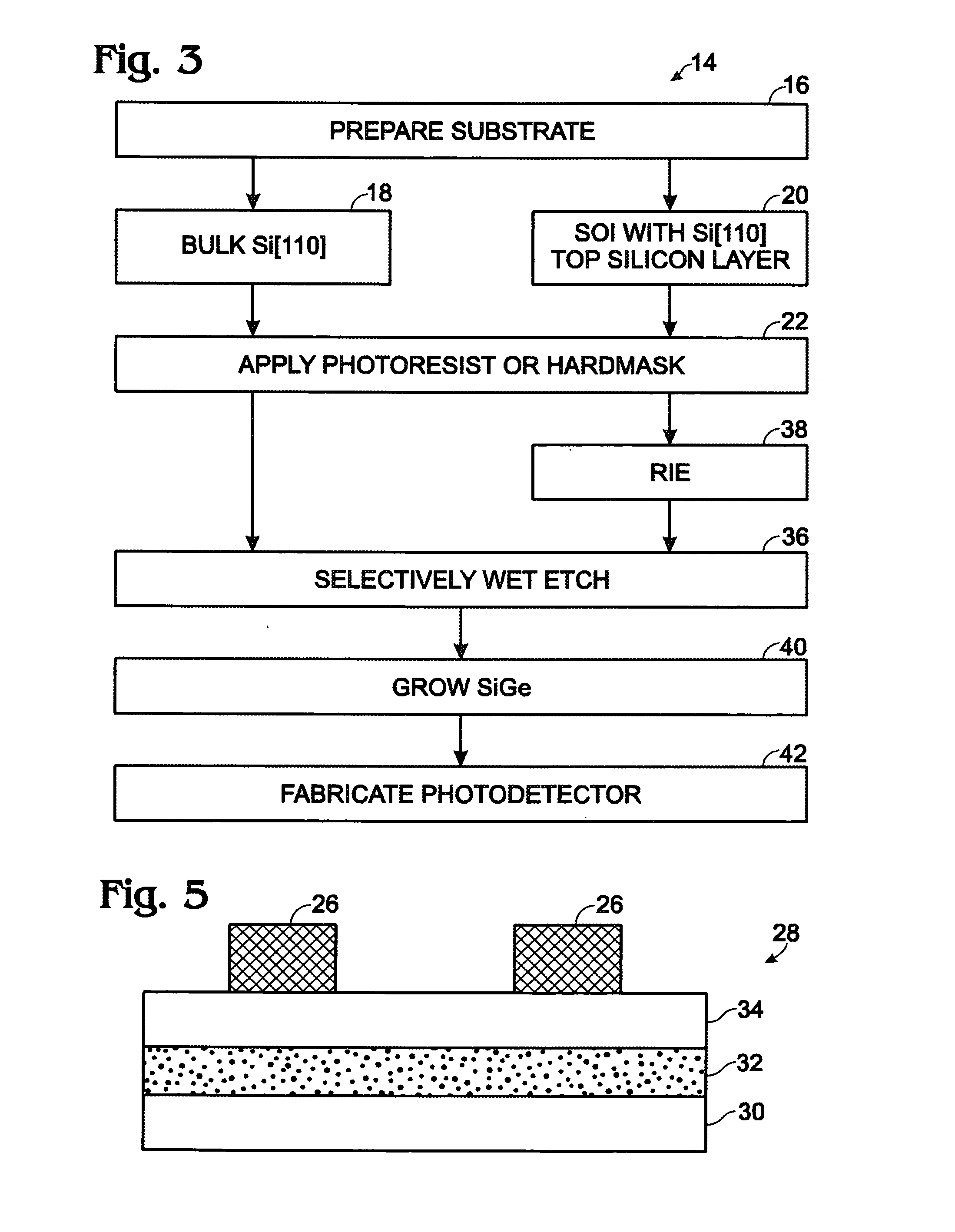
[0026] The objective of this invention is to improve the quantum efficiency of photodetectors, e.g., near-IR photodetectors, integrated on silicon substrates. This is done by providing silicon structures with nearly vertical sidewalls and low crystalline defects to enable the growth of low-defect strained, epitaxial SiGe and / or SiGe / Si multilayers on the sidewalls. By so doing, the optical path length for absorption of light is be determined by the height of the sidewalls, and not by the SiGe film thickness. In this way the quantum efficiency of the photodetector is improved.

[0027] As previously noted, the use of reactive ion-etching (RIE) to etch silicon structures results in rough, damaged sidewalls with unacceptably large slopes. The readily available selective etch processes do not improve this situation on silicon (001) substrates. The present invention uses silicon (110) substrates and selective chemical etching to fabricate vertical sidewalls on which to grow strained SiGe a...


PUM


Abstract

A method of fabricating vertical sidewalls on silicon (110) substrates for use in Si / SiGe photodetectors includes preparing a silicon (110) layer wherein the silicon (110) plane is parallel to an underlying silicon wafer surface. Masking the silicon (110) layer with mask sidewalls parallel to a silicon (111) layer plane and etching the silicon (110) layer to remove an un-masked portion thereof, leaving a patterned silicon (110) layer having vertical silicon (111) sidewalls. Removing the mask; growing SiGe-containing layers on the patterned silicon (110) layer; and fabricating a photodetector.

Description

FIELD OF THE INVENTION [0001] This invention relates to photodetectors, and particularly to near-infrared photodetectors integrated on silicon substrates. BACKGROUND OF THE INVENTION [0002] Photo detecting in the near infrared regime, i.e., having a wavelength of between 0.7 μm to 2 μm, has many applications, such as in fiber-optic communication, security applications, machine vision and night vision imaging. Although III-V compound semiconductors provide superior optical performance over their silicon-based counterparts, the compatibility of silicon based materials with current silicon-IC technology provides the possibility of making cheap, small and highly integrated optical systems. The following references provide additional background for the invention: Maiti et al., Strained Silicon Heterostructures: Materials and Devices, Chapter 10: Si / SiGe Optoelectronics, The Institution of Electrical Engineer, 2001; Murtaza et al., Room Temperature Electroabsorption in GexSi1-xPIN Photodi...

Claims


Application Information

Patent Timeline
Patent Type & Authority Applications(United States)
IPC IPC(8): H01L21/00
CPCY02E10/50H01L31/1812
Inventor TWEET, DOUGLAS J.LEE, JONG-JANMAA, JER-SHENHSU, SHENG TENG
Owner SHARP KK AKA SHARP CORP
Why Eureka
Try Eureka