

Method For Producing III Group Element Nitride Crystal, Production Apparatus For Use Therein, And Semiconductor Element Produced Thereby
a technology of iii group element and nitride crystal, which is applied in the direction of crystal growth process, polycrystalline material growth, crystal growth process, etc., can solve the problems of inconvenient processing and inferior quality, and achieve the effect of reducing the length of time required for crystals of a desired size, reducing the length of time required for supersaturation, and increasing the length of time required for substantial crystal growth
- Summary
- Abstract
- Description
- Claims
- Application Information
AI Technical Summary
Benefits of technology
Problems solved by technology
Method used
Image

Examples
embodiment 1
[0094] In this embodiment, GaN crystals are grown using Ga as a Group III element, a metal Na as alkali metal, and nitrogen (N2) gas as a nitrogen-containing gas. The description is directed to a method for growing the GaN crystals with reference to FIG. 7. FIG. 7 is a structural view showing an example of a configuration of an apparatus used in the producing method according to the present invention. As shown in the figure, this apparatus includes a pressure vessel 51, a gas supplying device 21, a flow amount adjuster 22, and a pressure adjuster 24 as main components. A reaction vessel 11 can be housed in the pressure vessel 51, and a heater 30 is disposed on a side face of the reaction vessel 11. The flow amount adjuster 22 and the pressure adjuster 24 are connected to the pressure vessel 51 via pipes, respectively, and the gas supplying device 21 is connected to the other end of the flow amount adjuster 22 via a pipe.
[0095] First, Ga and Na are put in the reaction vessel 11. The...
embodiment 2
[0096] In this embodiment, GaN crystals are grown using Ga as a Group III element, a metal Na as an alkali metal, and nitrogen (N2) gas as a nitrogen-containing gas. First, an ambient pressure and an ambient temperature are set to 60 atm to 70 atm (60×1.013×105 Pa to 70×1.013×105 Pa)(a pressure higher than an ambient pressure used during a time of crystal growth by, for example, 20 atm to 30 atm (20×1.013×105 Pa to 30×1.013×105 Pa)) and 850° C., respectively, and are kept for 1 hour to 5 hours so that nitrogen is allowed to dissolve rapidly in a melt containing Ga and Na to attain a desired nitrogen concentration in the melt (material preparation process). Then, in a state where the ambient temperature is kept at 850° C., the ambient pressure is lowered to 40 atm (40×1.013×105 Pa) so that GaN crystals are grown in the melt (crystal growth process). As a result, a length of time from a start of material heating to a start of crystal growth is reduced considerably to, for example, 10 ...
embodiment 3
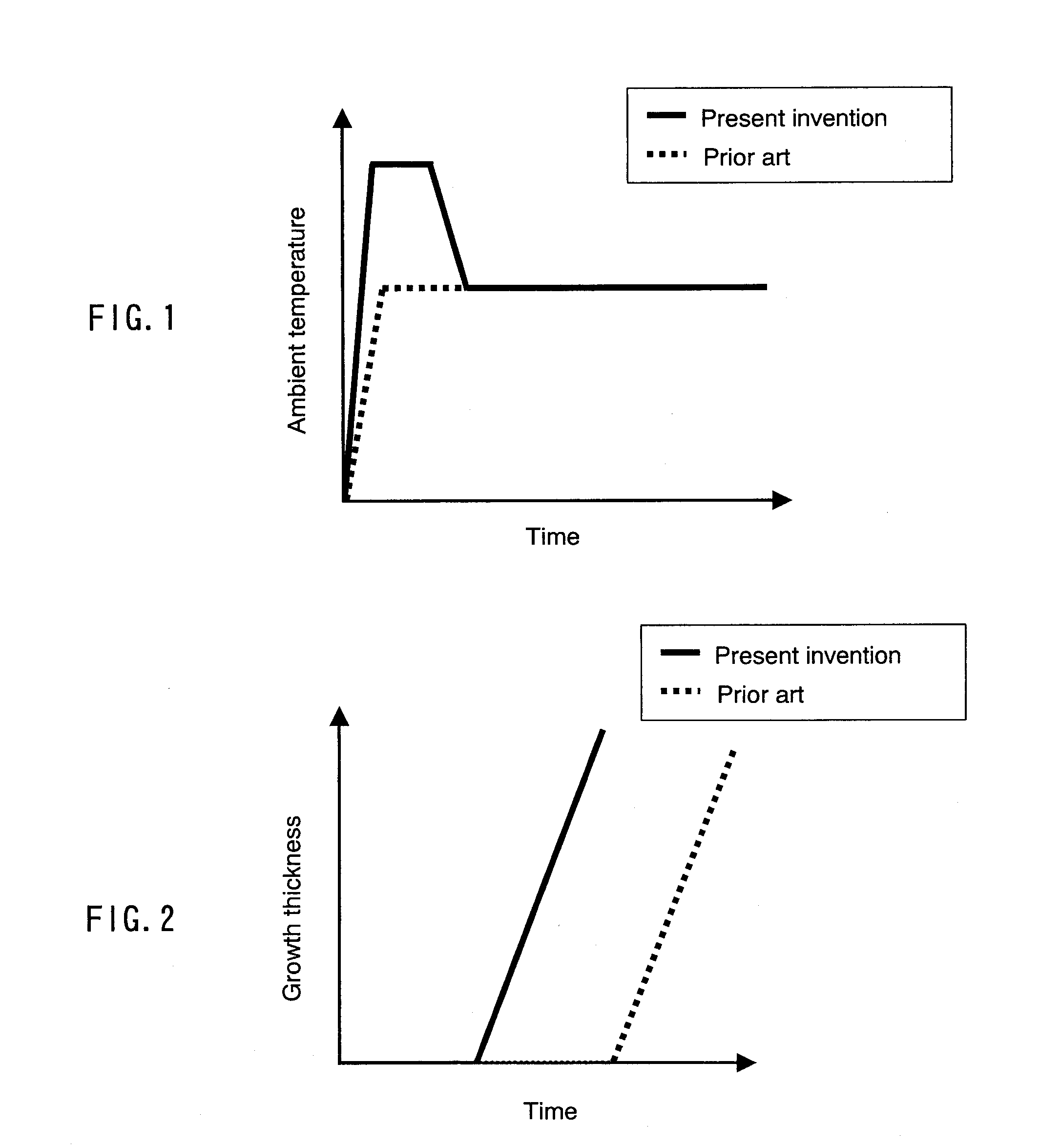
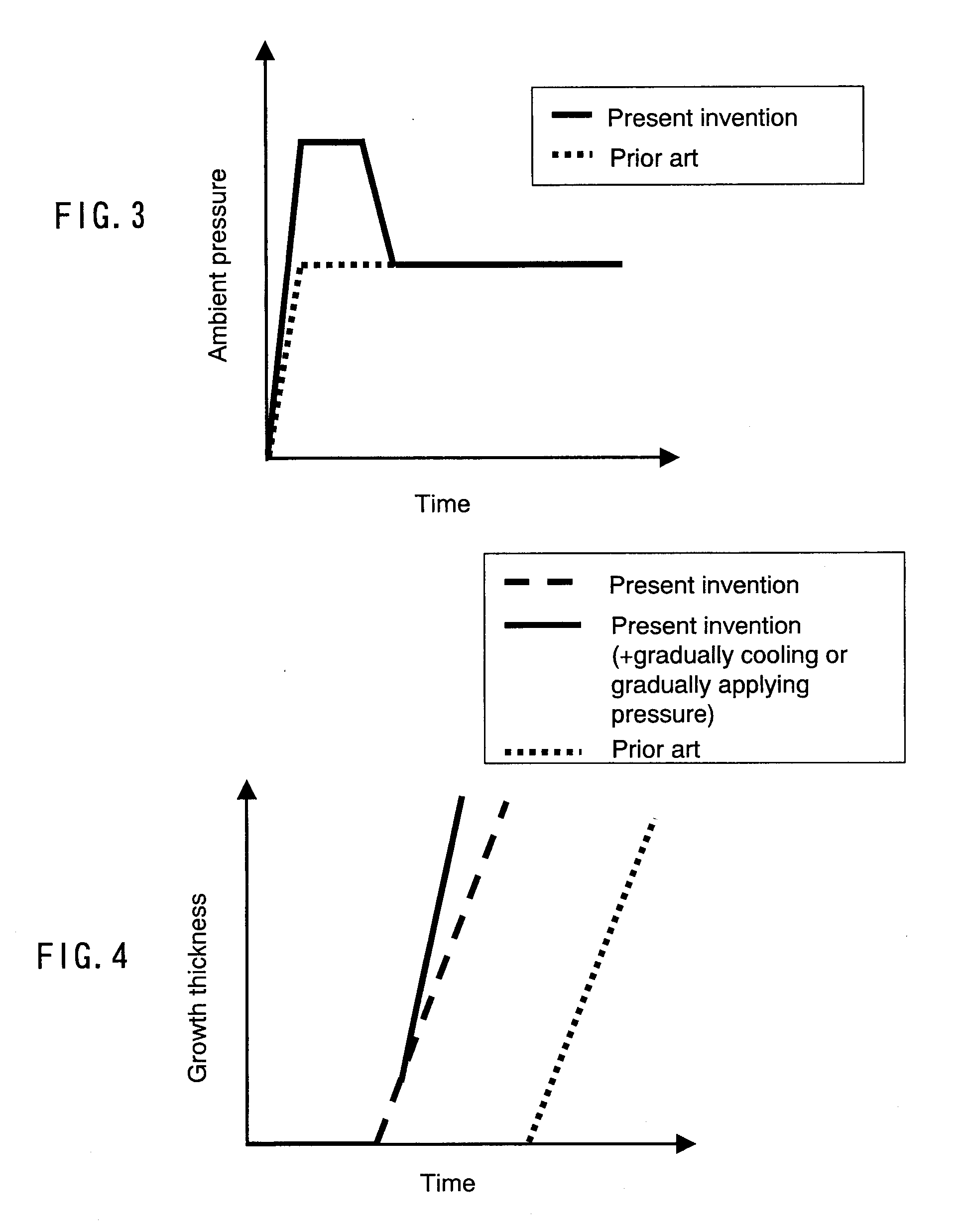
[0097] In this embodiment, first, a material preparation process is performed in the same manner as in Embodiment 1, and an ambient temperature is lowered. Then, in a crystal growth process, the ambient temperature further is lowered at a rate of 0.2° C. per hour to 1.5° C. per hour. As a result, a substantial crystal growth rate further is increased and can be, for example, 25 μm per hour. FIG. 5 shows an example of a change over time in ambient temperature in this embodiment, and FIG. 4 shows an example of a relationship between growth thickness and time in this embodiment. FIG. 4 also shows a relationship between growth thickness and time in the case where crystals are grown by the conventional method. An ambient temperature is not particularly required to be lowered linearly with respect to time and may be lowered in a step-wise manner. Further, an ambient temperature may be lowered at a rate gradually increasing in a range of, for example, 0.1° C. per hour to 1.5° C. per hour. ...
PUM
| Property | Measurement | Unit |
|---|---|---|
| pressure | aaaaa | aaaaa |
| pressure | aaaaa | aaaaa |
| temperature | aaaaa | aaaaa |
Abstract
Description
Claims
Application Information