Piezo-diode cantilever MEMS

a diode and diode technology, applied in the direction of microstructural devices, acceleration measurement using interia forces, instruments, etc., can solve the problems of changing electrical current and strain across a large surface area to create current changes, and achieve enhanced mechanical strain, enhanced chemical vapor deposition, and reduced mems

Inactive Publication Date: 2007-12-06
SHARP KK
View PDF5 Cites 22 Cited by
  • Summary
  • Abstract
  • Description
  • Claims
  • Application Information

AI Technical Summary

Benefits of technology

[0019] Sensitivity and signal-to-noise ratio are two important parameters for MEMS sensors. The present invention piezo-diode cantilever MEMS sensor converts mechanical energy (surface stress) induced on a molecule-solid interface to electrical energy. Reducing the MEMS structure thickness effectively enhances the mechanical strain induced by surface stress. In one aspect, the present invention uses a plasma enhanced chemical vapor deposition (PECVD) method to control the MEMS structure thickness, and uses a pre-deposited sacrifici...

Problems solved by technology

If the P-I-N diode is fabricated on an amorphous film, the mechanical strain change on the amorphous film affects its current transport mechanism in the diode, resulting in a change in ...

Method used


Image

  • Piezo-diode cantilever MEMS
  • Piezo-diode cantilever MEMS
  • Piezo-diode cantilever MEMS

Examples


Embodiment Construction

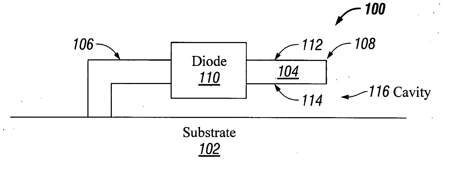
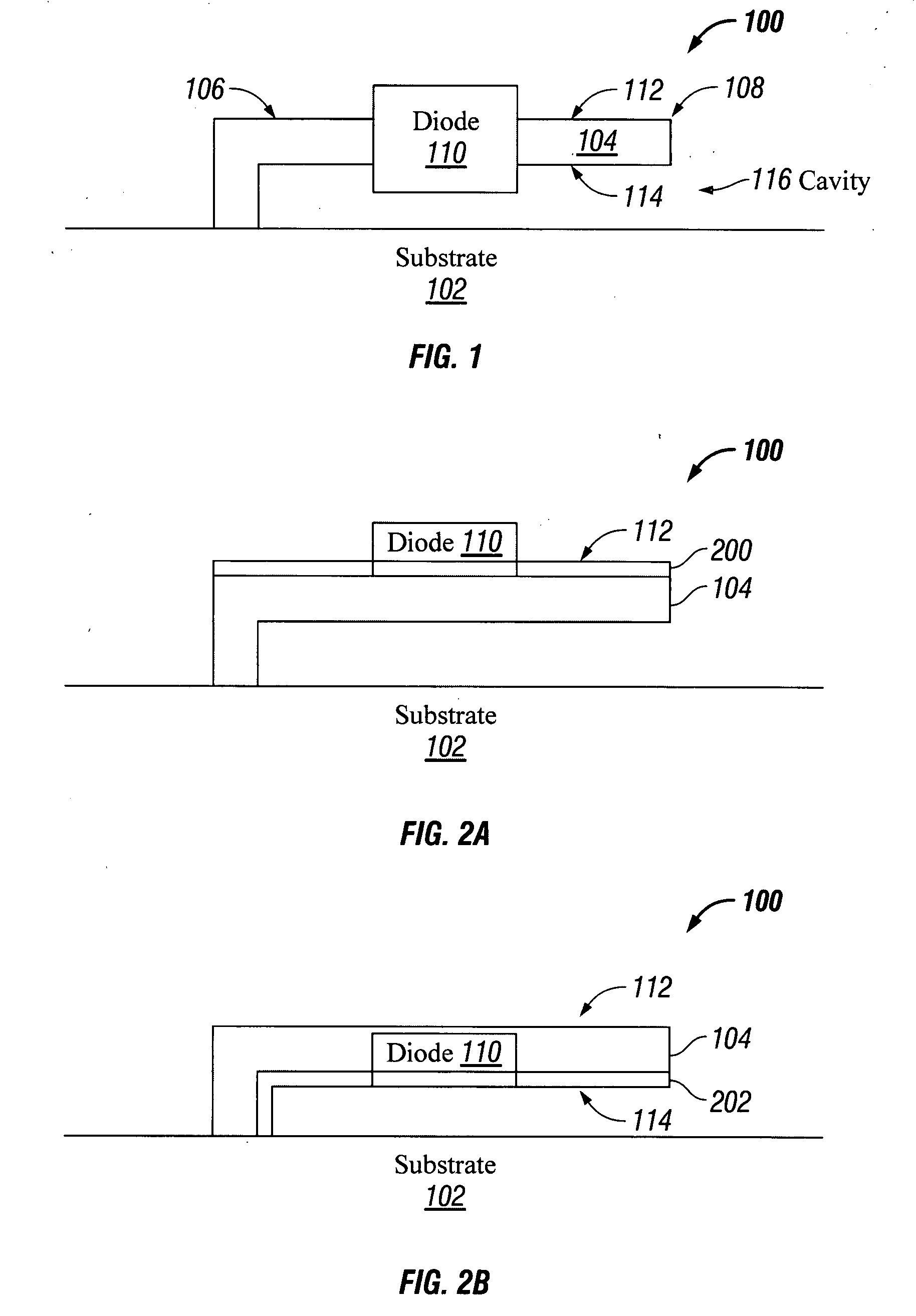
[0033]FIG. 1 is a partial cross-sectional view of a piezo thin-film diode (piezo-diode) cantilever microelectromechanical system (MEMS). The piezo-diode cantilever 100 comprises a substrate 102. Some possible substrate materials include glass, polymer, quartz, metal foil, Si, Si-containing materials, sapphire, ceramic, and compound semiconductor materials, such as Si-germanium for example. A multi-layered film cantilever beam 104 has a distal end 106 anchored to the substrate 102, and a proximal end 108. A diode 110 is embedded in the cantilever beam 104 and shares a film layer in common with the cantilever beam 104. The cantilever beam 104 has a top surface 112 and a bottom surface 114. A cavity 116 is formed between the cantilever beam proximal end 108 and the substrate 102.

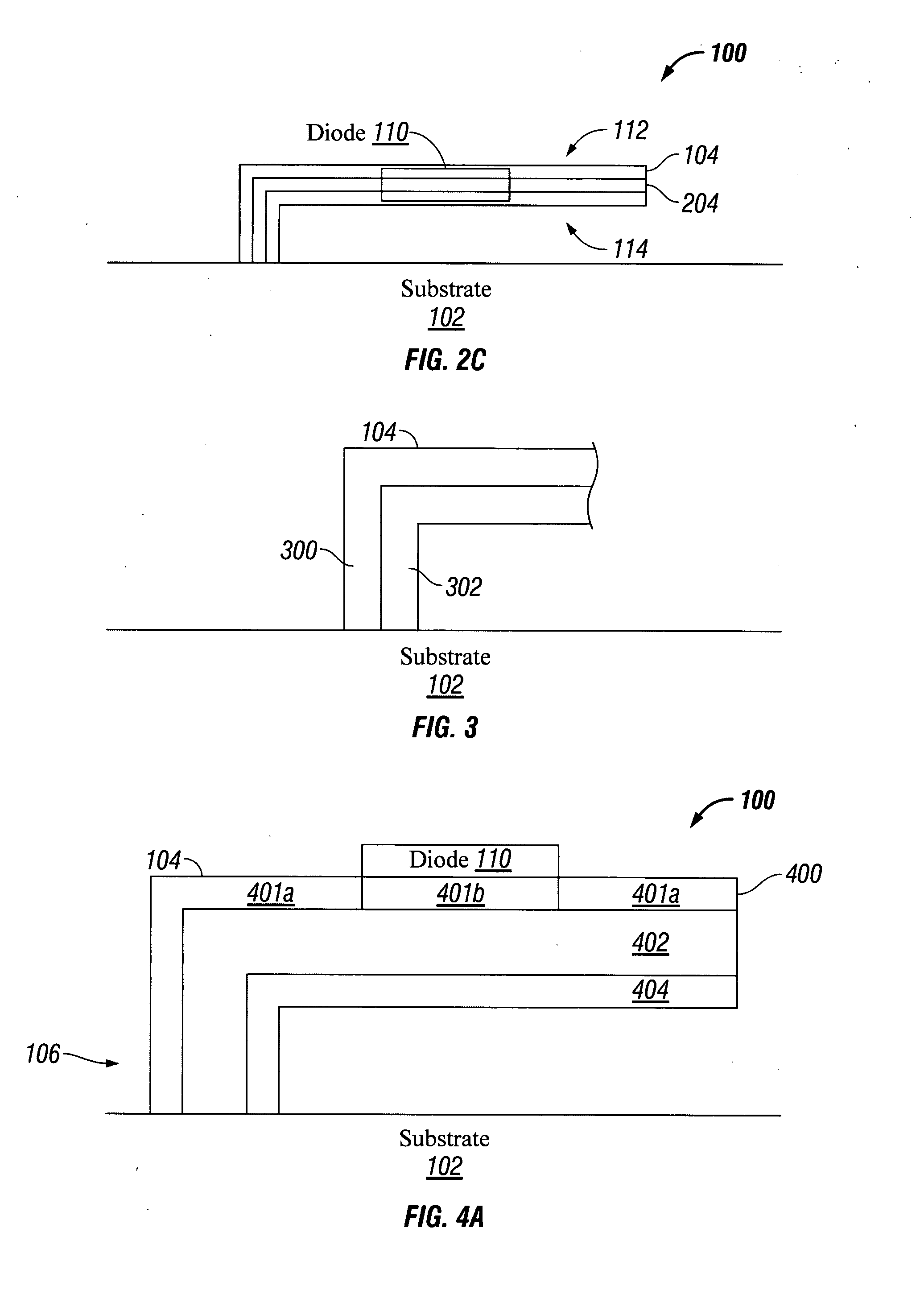
[0034] The cantilever body can be a rectangular as shown, or shaped (e.g., as a triangle, circle, or oval), with one or multiple points for anchoring to the substrate. The cantilever beam 104 and diode 110 fil...


PUM


Abstract

A piezo thin-film diode (piezo-diode) cantilever microelectromechanical system (MEMS) and associated fabrication processes are provided. The method deposits thin-films overlying a substrate. The substrate can be made of glass, polymer, quartz, metal foil, Si, sapphire, ceramic, or compound semiconductor materials. Amorphous silicon (a-Si), polycrystalline Si (poly-Si), oxides, a-SiGe, poly-SiGe, metals, metal-containing compounds, nitrides, polymers, ceramic films, magnetic films, and compound semiconductor materials are some examples of thin-film materials. A cantilever beam is formed from the thin-films, and a diode is embedded with the cantilever beam. The diode is made from a thin-film shared in common with the cantilever beam. The shared thin-film may a film overlying a cantilever beam top surface, a thin-film overlying a cantilever beam bottom surface, or a thin-film embedded within the cantilever beam.

Description

RELATED APPLICATIONS [0001] This application is a continuation-in-part of a pending patent application entitled, PIEZO-TFT CANTILEVER MEMS, invented by Zhan et al., Ser. No. 11 / 031,320, filed Jan. 5, 2005, Attorney Docket No. SLA954, which is a continuation-in-part of the following six applications: [0002] CRYSTAL-STRUCTURE-PROCESSED MECHANICAL DEVICES AND METHODS AND SYSTEMS FOR MAKING, invented by John Hartzell, Ser. No. 10 / 131,318, filed Apr. 23, 2002, attorney docket no. SLA685, now U.S. Pat. No. 7,125,451; [0003] THIN-FILM CRYSTAL-STRUCTURE-PROCESSED DEVICES AND METHODS AND SYSTEMS FOR MAKING, invented by John Hartzell, Ser. No. 10 / 131,006, filed Apr. 23, 2002, attorney docket no. SLA686, now U.S. Pat. No. 7,128,783; [0004] SEMICONDUCTOR CRYSTAL-STRUCTURE-PROCESSED MECHANICAL, AND METHODS AND SYSTEMS FOR MAKING, invented by John Hartzell, Ser. No. 10 / 131,057, filed Apr. 23, 2002, attorney docket no. SLA687, now U.S. Pat. No. 6,860,939; [0005] MONOLITHIC INTEGRATED CRYSTAL-STRUC...

Claims


Application Information

Patent Timeline
IPC IPC(8): H01L29/84H01L21/02
CPCH01L29/868B81B3/0021
Inventor ZHAN, CHANGQINGSCHUELE, PAUL J.CONLEY, JOHN F. JR.HARTZELL, JOHN W.
Owner SHARP KK
Why Eureka
Try Eureka