Optical device and method of manufacture

Inactive Publication Date: 2007-12-13
OPTAGLIO
View PDF13 Cites 44 Cited by
  • Summary
  • Abstract
  • Description
  • Claims
  • Application Information

AI Technical Summary

Benefits of technology

[0020] Advantageously, the combination of this data pre-processing methodology and a new flexible e-beam writing technique can be combined to form a new arrangement and system for the exact direct digital recording of any holographic or diffraction grating structure by electron beam writing of the pattern into, for example, silicon. Such an arrangement allows essentially a nearly unlimited flexibility with regard to the microstructure that can be recorded allowing an enormous range of optical structures to be recorded and combined together with a diverse range of characteristics (straight lines, continuous curved lines, geometrical shapes), and both diffraction grating. Fourier hologram and rainbow hologram patterns and optical element patterns can be recorded into one hologram.
[0021] Furthermore the resolution of graphical motifs achievable in accordance with the present invention equates to the resolution of the microstructure of the hologram itself and these patterns can be drawn continuously and without recourse to previous techniques which involve splitting graphic designs into line and pixel patterns to record difference effects.
[0022] Within the concept of the present invention there is co

Problems solved by technology

Such diffractive, optically variable image forming devices are used as anti-counterfeit devices both because their effects are highly recognizable and cannot be duplicated by print technologies, and because specific, and difficult-to-replicate, optical and engineering techniques are required for their production.
It should be noted that all of the above techniques are limited to subdividing images into rectangular pixels that generally contain diffraction gratings of various types.
A disadvantage of the ‘Pixelgram’ image p

Method used


Image

  • Optical device and method of manufacture
  • Optical device and method of manufacture
  • Optical device and method of manufacture

Examples


Embodiment Construction

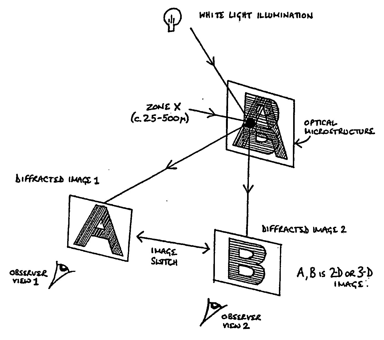
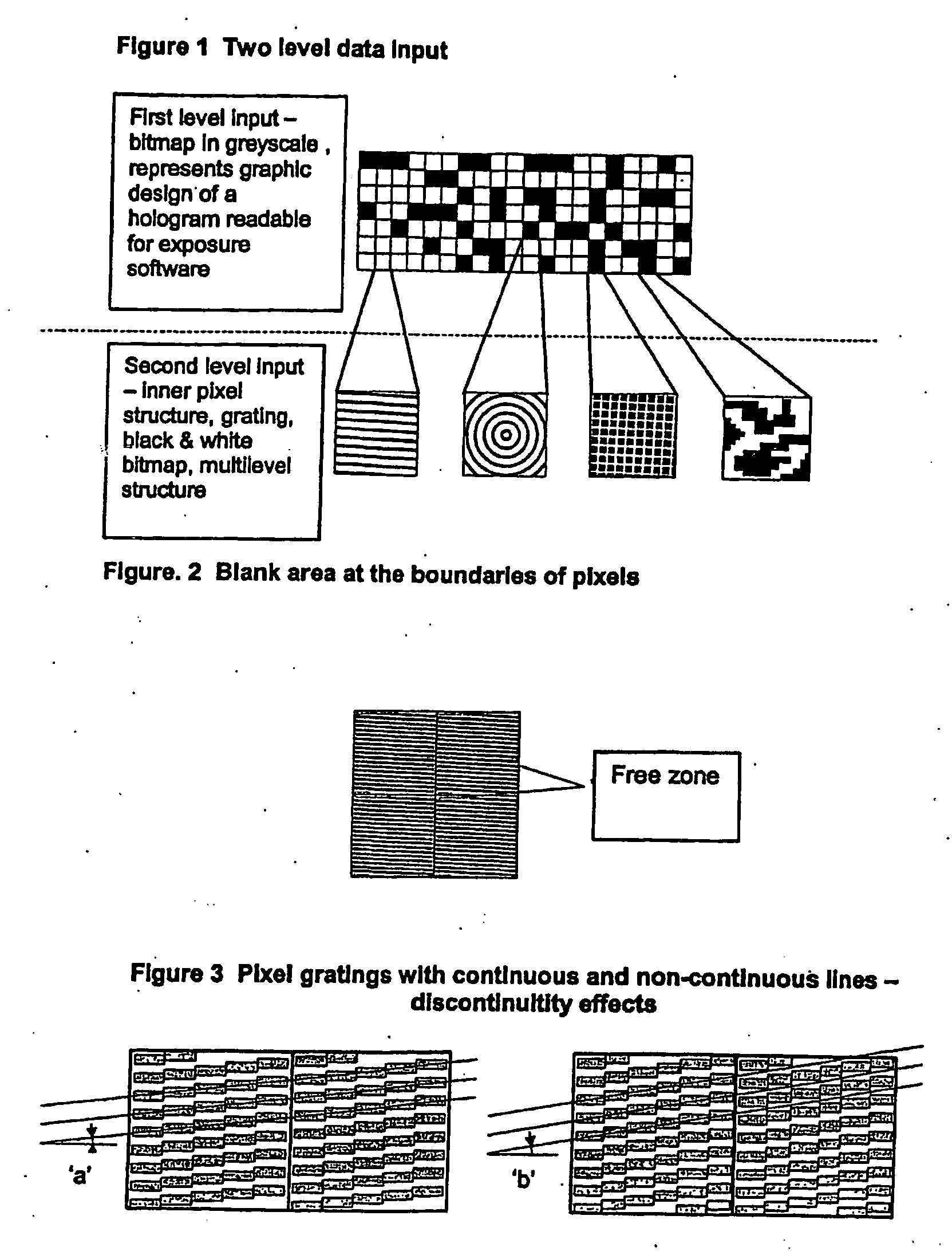
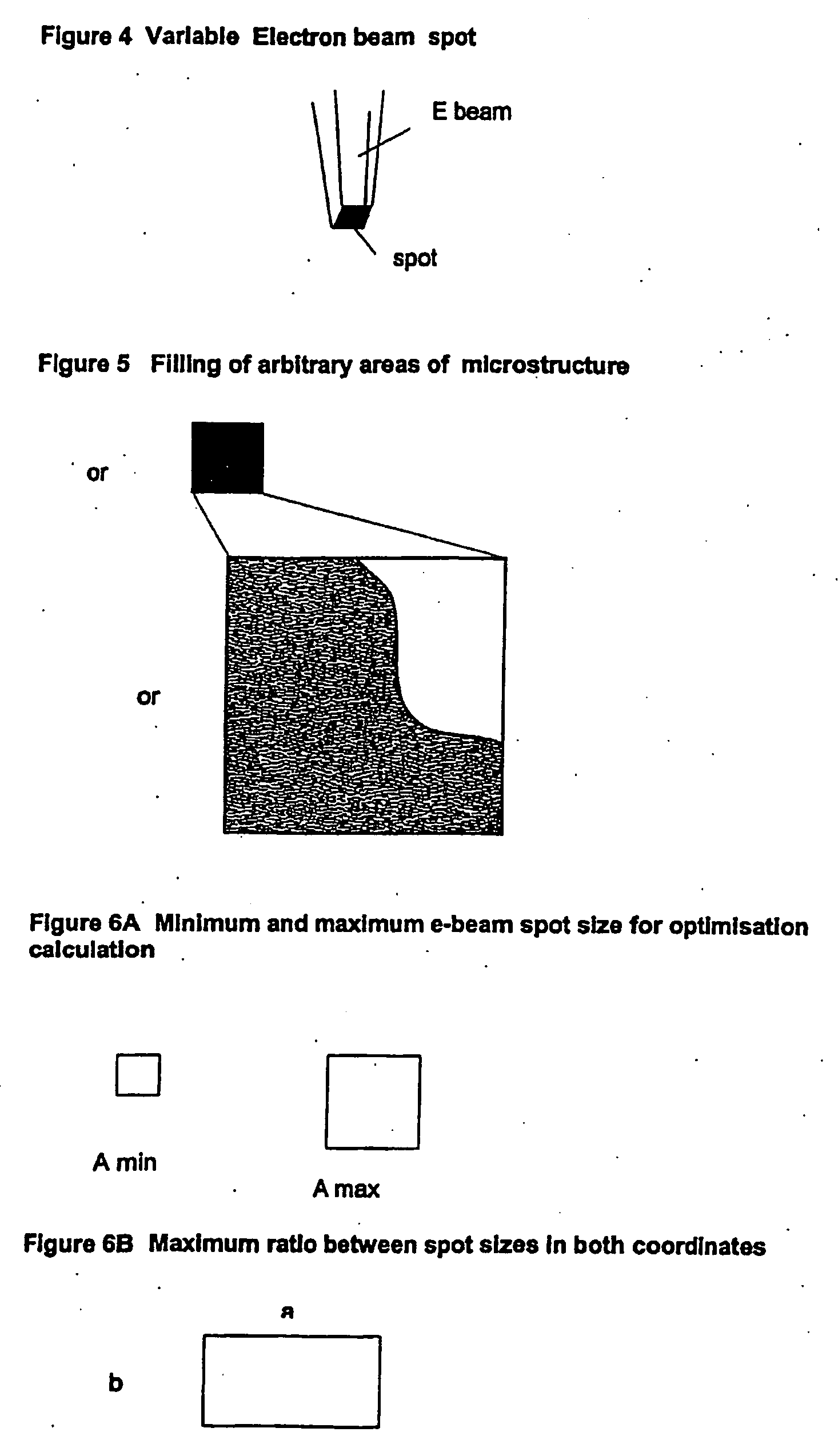
[0054] Throughout the text, it should be appreciated that the process of forming an embossed hologram or embossed surface relief diffractive structure is broadly as known in the art (e.g. G. Saxby, “Practical Holography’) after the lithographic exposure step. To form an embossed hologram the surface relief image exposed by the lithograph after development is formed in photo-resist—this is would be silvered to deposit a conductive layer, copied probably several times in a plating process as known in the field to form metal copies of the structure and then typically roll embossed into a plastic material or embossing lacquer or hot foil material using a thermo forming process, or cast into an ultra violet curable material and then metallised with typically aluminum or another reflective metal, perhaps chromium for example, to form an embossed hologram or embossed surface relief diffractive structure as known in the art. In an alternative process the surface relief diffractive structure...


PUM


Abstract

The present invention provides for a method of producing an optical device by means of electron beam lithography and including the step of varying the characteristics of the electron beam spot during formation of the device and also an apparatus for producing diffractive optical devices and/or holographic devices by means of electron beam lithography and including an electron beam lithograph, controlling and processing means, means for varying the characteristics of the electron beam spot during formation of the device, and wherein the processing means is arranged for compiling and pre-processing data and for providing optimisation and allocation control and to optical devices such as those produced thereby.

Description

[0001] This application is a continuation application and claims the benefit of U.S. patent application Ser. No. 10 / 483,840, filed Jul. 16, 2004, entitled “OPTICAL DEVICE AND METHOD OF MANUFACTURE”, which in turn claims the benefit of PCT / GB / 02 / 03257, filed Jul. 16, 2002, which in turn claims priority to application UK 0117391.3, filed Jul. 17, 2001, the complete disclosures of which are incorporated herein by reference.BACKGROUND OF THE INVENTION [0002] This invention relates to optical devices and related methods of manufacture and verification. In particular, but not exclusively, the invention relates to security anti-counterfeit devices employing the principle of optical diffraction, and to an improved form of optical security device for use in the protection of documents and articles of value from counterfeit and to verify authenticity. [0003] Several forms of such devices are known and used to prove the authenticity of items of value and to prevent their fraudulent duplication...

Claims


Application Information

Patent Timeline
IPC IPC(8): G02B27/42G06K19/16G06K1/00B42D15/10G03H1/30
CPCB42D2035/14B42D2035/16B42D2035/44G03H1/0244G03H1/028G03H1/265Y10T428/315G03H2001/0497G03H2001/303G03H2001/048B42D25/29B42D25/342B42D25/328G03H1/30G03H1/0236G03H2210/55G03H2224/04G03H2230/10B42D25/324B42D25/425
Inventor RYZI, ZBYNEKDRINKWATER, KENNETH JOHNMATEJKA, FRANTISEK
Owner OPTAGLIO
Why Eureka
Try Eureka