This helps you quickly interpret patents by identifying the three key elements:
Problems solved by technology
Method used
Benefits of technology
Benefits of technology
[0012]It is a third object of the invention to provide methods of producing poly(organo siloxane) compositions, which are suitable for the preparation of thin films having excellent dielectric properties and optical properties.
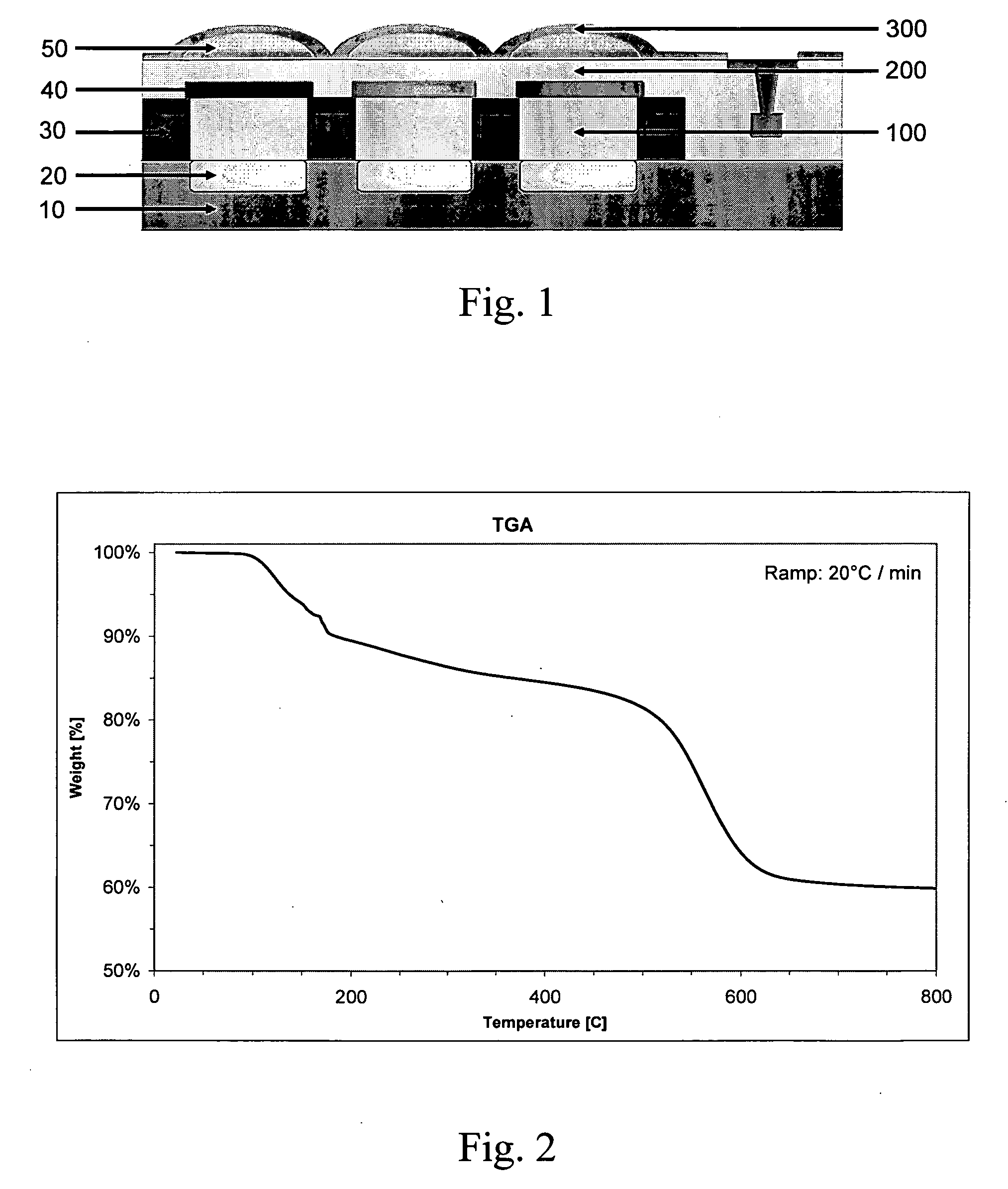
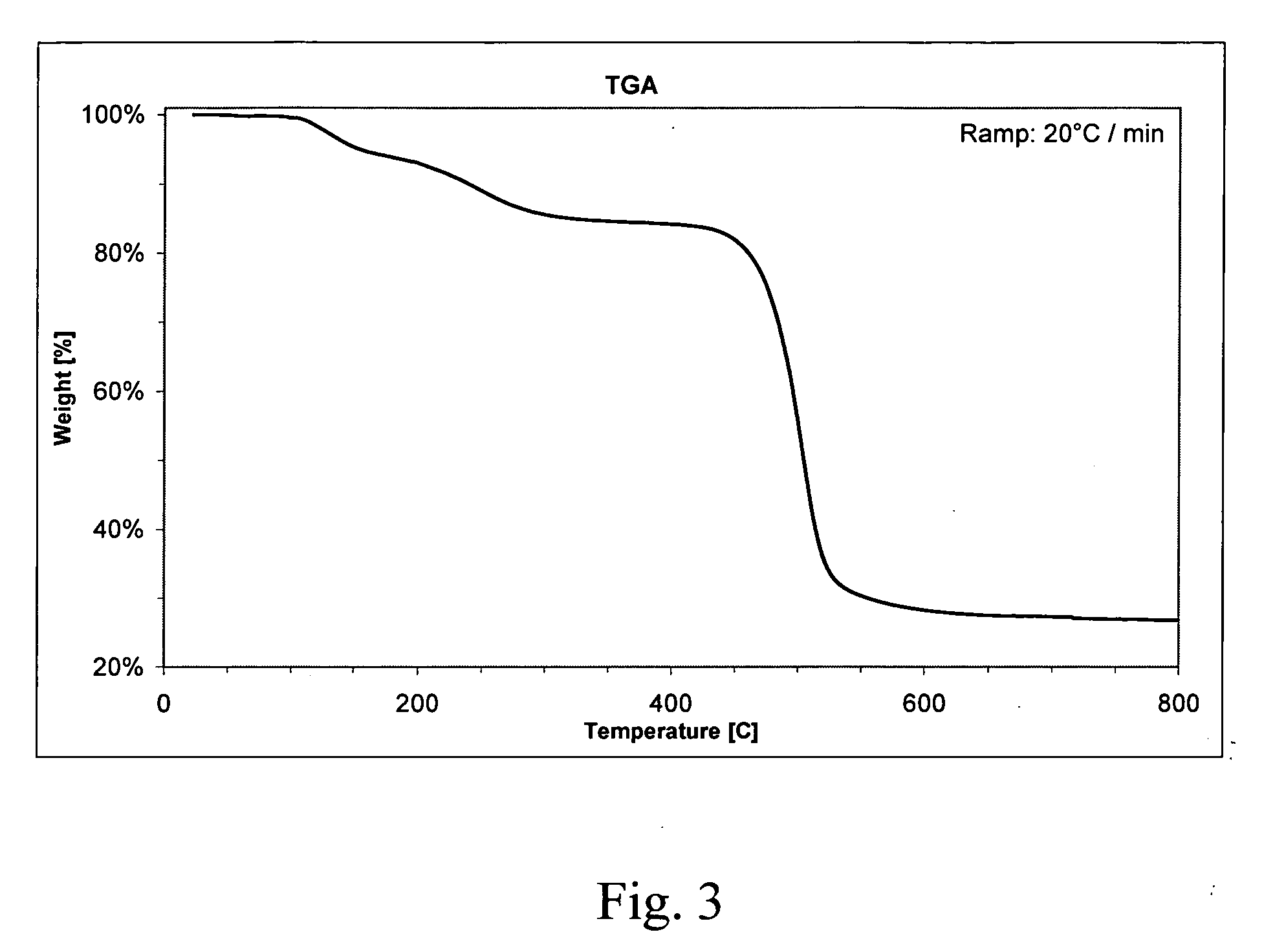
[0034]By incorporating nanoparticles into the materials comprising a disilane structure having optionally functional groups the refractive index which is already high compared with conventional siloxane materials (about 1.65 compared to <1.5) can be even improved and values in the range of up to 1.75 or even higher can be attained which makes the novel materials particularly attractive for CMOS camera applications.
Problems solved by technology
However, applicability of these films is limited because of their low thermal stability, softness, and incompatibility with traditional technological processes developed for SiO2 based dielectrics.
For example, organic polymer cannot be chemical mechanical polished or etched back by dry processing without damaging the film.
However, these organic units reduce the degrees of bridging crosslinks as well increases the free volume between the molecules due to steric hindrance.
Method used
Image
Click on the blue label to locate the original text in one second.
Reading with bidirectional positioning of images and text.
Examples
example 1
1,1,1,4,4-Pentachloro-1,4-disilabutane (The Intermediate)
[0111]
[0112]Vinyltrichlorosilane (68.8 g, 426 mmol) and cobalt octacarbonyl (700 mg) were placed in a 100 mL rb flask and cooled in an ice bath to 0° C. Dichlorosilane (bp. 8° C., 44.3 g, 439 mmol) was then condensed into the flask, The system was allowed to warm up to room temperature during night. Distillation at 60 . . . 62° C. / 8 mbar gave 1,1,1,4,4-Pentachloro-1,4-disilabutane (120.8 g, 460 mmol) in 93% yield.
[0114]11.00 g (0.076 mol) trivinylchlorosilane was added to a 100 ml vessel followed by 2 ml 1,1,1,4,4-pentachloro-1,4-disilabutane. The solution was heated to 80° C. and 15 μL of a 10% H2PtCl6 / IPA-solution was added. Strong exothermic reaction was observed and heat was switched off. Rest of 1,1,1,4,4-pentachloro-1,4-disilabutane was added slowly during 30 min keeping the temperature of the solution below 130° C. The total amount of 1,1,1,4,4-pentachloro-1,4-disilabutane was 61.50 g (0.234 mol, 2.6% excess). After addition heat was again switched on and solution was stirred for an hour at 110° C. After that solution was distilled yielding 47.08 g (66%) tris(3,3,6,6,6-pentachloro-3,6-disilahexyl)chlorosilane. B.p. 264° C. / <0.5 mbar.
example 3
1,1,1,4,4,7,7,7-Octachloro-1,4,7-trisilaheptane
[0115]
[0116]Vinyltrichlorosilane (16.8 g, 104 mmol) was heated to 60° C. and 100 μL 10% H2PtCl6 / IPA-solution was added. 1,1,1,4,4-pentachloro-1,4-disilabutane (20.4 g, 77.7 mmol) was added slowly during 20 min so that the temperature did not exceed 100° C. The reaction was allowed to proceed for 12 hours at 100° C., after which it was distilled under vacuum at 115-130° C. / <1 mbar. The yield was 31.5 g (74.3 mmol, 96%).
PUM
Abstract
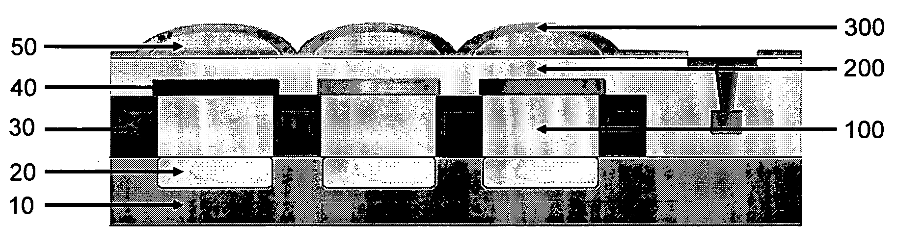
A semiconductor device comprising a semiconductor substrate with a plurality of photo-diodes arranged in the semiconductor substrate with interconnect layers defining apertures at the photo-diodes and a first polymer which fills the gaps such as to cover the photo-diode. Further, layers of color filters are arranged on top the gap fillingpolymer layer opposite to the photo-diodes and a second polymer arranged on the interconnect layers covers and planarizes and passivates the color filter layers. On top of the planarizing polymer there is a plurality of micro-lenses opposite to the color filters, and a third polymer layer is deposited on the micro-lenses for passivating the micro-lenses. According to the invention the polymer materials are comprised of a siloxane polymer which gives thermally and mechanically stable, high index of refraction, dense dielectric films exhibiting high-cracking threshold, low pore volume and pore size.
Description
[0001]This application claims priority of U.S. Provisional Patent Application Ser. No. 60 / 812,958 filed Jun. 13, 2006, which is incorporated herein by reference.BACKGROUND OF THE INVENTION[0002]1. Field of the Invention[0003]The present invention relates to a process for making semiconductor devices by utilizing novel polymers. In particular, the invention provides novel semiconductors in which at least one layer optical or electrical of CMOS image sensors is made utilizing a polymer or polymer compositions of functionalized silane monomers. Further, the invention concerns integrated circuit and optoelectronic devices and methods of processing novel polymer materials in manufacturing them.[0004]2. Description of Related Art[0005]The commercial use of electronic image sensors in electronics has increased dramatically over the last few years. They are found in cameras, cell phones, and are used for new safety features in automobiles e.g. for estimating distances between vehicles, dete...
Claims
Application Information
Patent Timeline
Application Date:The date an application was filed.
Publication Date:The date a patent or application was officially published.
First Publication Date:The earliest publication date of a patent with the same application number.
Issue Date:Publication date of the patent grant document.
PCT Entry Date:The Entry date of PCT National Phase.
Estimated Expiry Date:The statutory expiry date of a patent right according to the Patent Law, and it is the longest term of protection that the patent right can achieve without the termination of the patent right due to other reasons(Term extension factor has been taken into account ).
Invalid Date:Actual expiry date is based on effective date or publication date of legal transaction data of invalid patent.

