
Photomask and exposure method

Active Publication Date: 2007-12-13
PANASONIC SEMICON SOLUTIONS CO LTD +1
View PDF8 Cites 9 Cited by
  • Summary
  • Abstract
  • Description
  • Claims
  • Application Information

AI Technical Summary

Benefits of technology

[0049] The aforementioned light-shading film prevents the aforementioned adhesives and the remaining component from being irradiated with this stay light, thus consequently preventing gas generation from the adhesive, being the organic matter, and reducing an adhesion of the deposit onto the photomask.
[0050] Particularly, the deposit is suitably prevented from generating and adhering onto the photomask, in the photomask used in the exposure apparatus using a high output laser beam with a wavelength of 200 nm or less as the light source of the exposure light, namely, the photomask easily allowing the deposit to be generated on the photomask.

Problems solved by technology

However, in the photomask, with the transfer pattern formed thereon by using the negative resist, namely, the photomask, with the non-drawing region, namely the transparent substrate exposed in the peripheral region of the main region excluding the desired mark pattern and the light-shading band, there occurs a problem that a plurality of foreign matters are found in the photomask after use.
Accordingly, regarding the photomask with the transfer pattern formed thereon by using the negative resist, namely, the photomask, with the non-drawing region, namely, the transparent substrate exposed in the peripheral region of the main region excluding a desired mark pattern and the light-shading band, there is a problem that the photomask becomes unusable with a few using times.
Therefore, there is a problem that even more foreign matters could be generated, as the exposure light wavelength applied by the exposure apparatus becomes shorter, accompanied by applying finer LSI pattern in recent years.

Method used


Image

  • Photomask and exposure method
  • Photomask and exposure method
  • Photomask and exposure method

Examples


example

[0090] This example shows an example of applying the present invention to the halftone phase shift mask.

[0091] Namely, as shown in FIGS. 4A-4G, in the photomask of this example, a photomask blank 15 is prepared by firstly forming a light semi-transmitting film 12 of a single film structure substantially consisting of metal such as molybdenum, silicon, and nitrogen on the transparent substrate 2, forming a chromium-based light shading film 13 thereon, and further forming a negative resist film 14 thereon (FIG. 4A).

[0092] The aforementioned light semi-transmitting film 12 is formed by using a mixture target (Mo:Si=8:92 mol %) of the molybdenum (Mo) and silicon (Si), in a mixture gas atmosphere (Ar:N2=10%:90%, pressure: 0.2 Pa) of argon (Ar) and nitrogen (N2), by reactive sputtering (DC sputtering), on the transparent substrate 2. This photomask blank 15 is an ArF excimer laser photomask blank with transmittance of about 5.5% and phase shift amount of about 180 deg, in the ArF excime...


PUM


Abstract

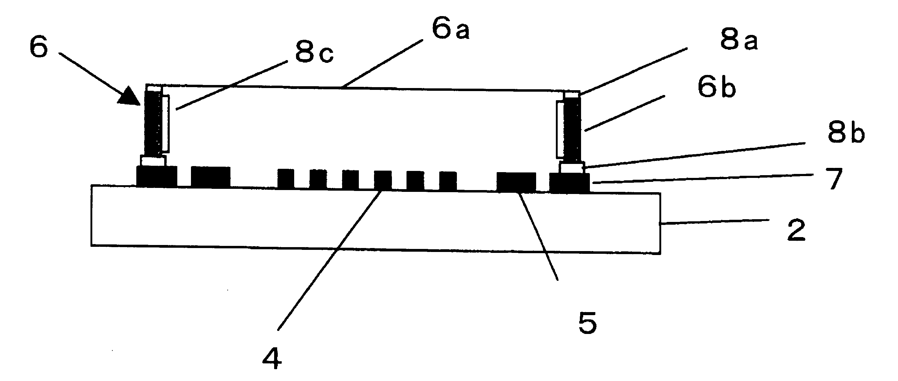
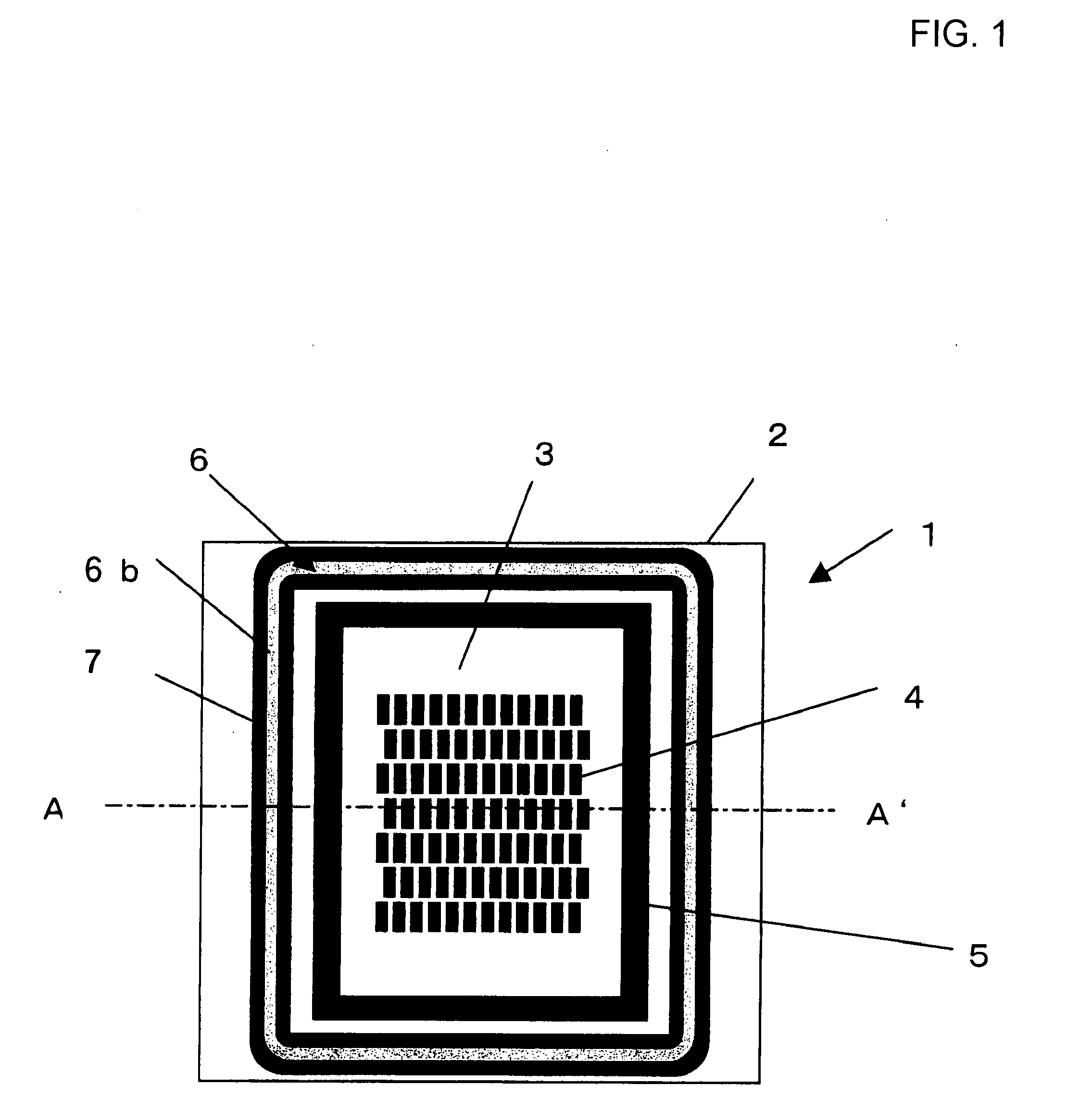
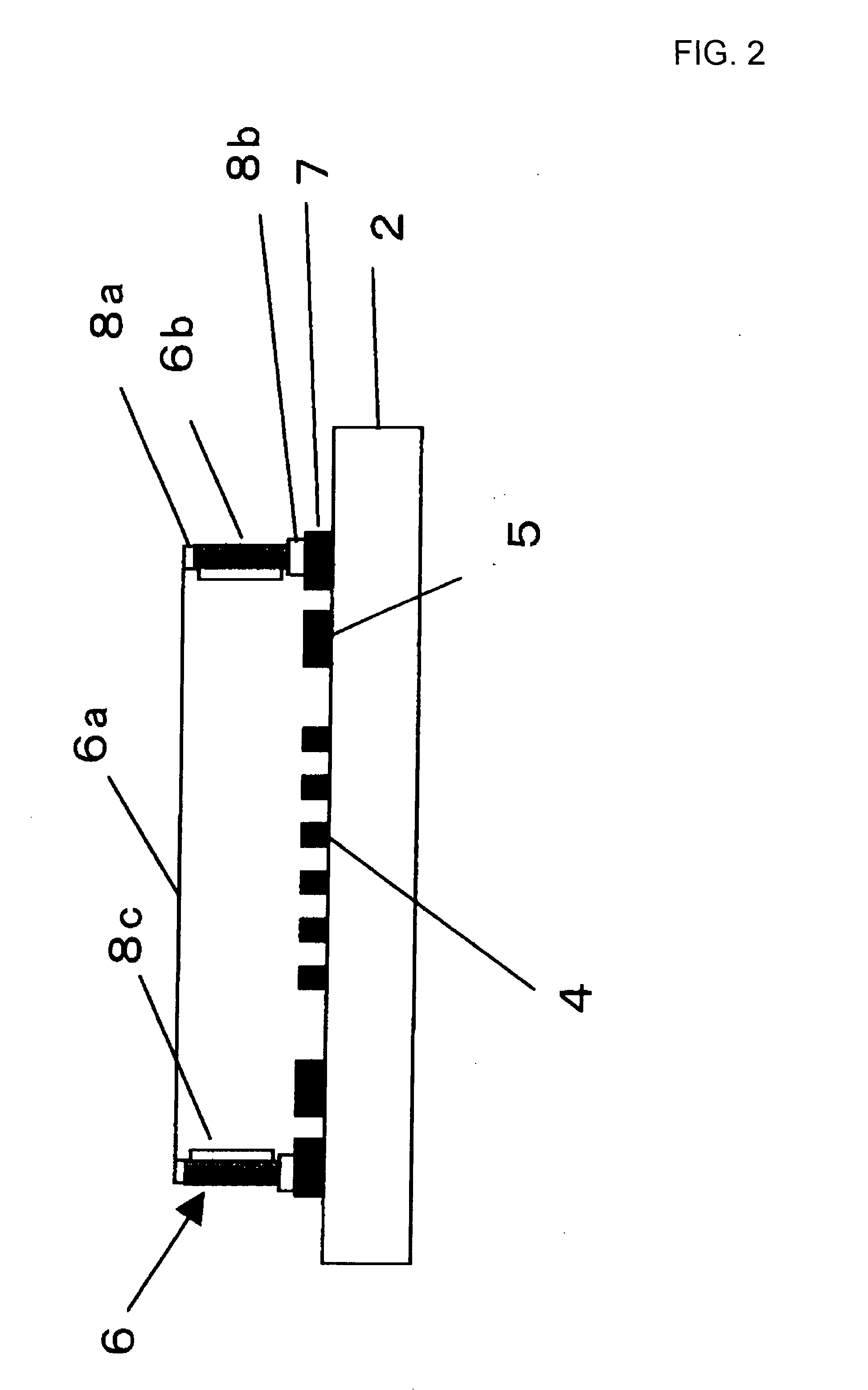
To provide a photomask capable of preventing a foreign matter generation in using the photomask, and an exposure method using this photomask. The photomask includes a transparent substrate 2; a transfer pattern 4 formed in a main region 3 of a center portion of the transparent substrate 2; a light-shading band region 5 provided adjacent to the main region 3 in the outer peripheral region of the main region 3; and a pellicle 6 formed by adhering a pellicle film 6a to a pellicle frame 6b by an adhesive 8a, wherein this pellicle 6 is adhered onto a light-shading region 7 consisting of a light-shading film formed in the outer peripheral region of the main region 3, through an adhesive 8b.

Description

TECHNICAL FIELD [0001] The present invention relates to a photomask used for a pattern transfer using an exposure apparatus and an exposure method using this photomask, in a manufacture of a semiconductor device. BACKGROUND ART [0002] Irradiation of exposure light is performed through a photomask (reticle), for example, to form a transfer pattern in a manufacture of the semiconductor device. [0003] A photomask formed with a light-shading film pattern on a transparent substrate composed of a rectangular quartz glass is conventionally used, and as a material of a light-shading film, a chromium-based material (elementary chromium, or chromium containing nitrogen, oxygen, and carbon, etc, or a lamination film of these material films) is generally used. [0004] Further, in recent years, a phase shift mask has been developed for practical use, to improve a resolution of the transfer pattern. Various types (for instance, a Levenson-type, an assist-pattern-type, and a self-matching type, etc...

Claims


Application Information

Patent Timeline
IPC IPC(8): A47G1/12G03F1/14G03F1/00G03F1/32G03F1/62G03F1/64G03F1/68
CPCG03F1/64G03F1/62G03F1/32
Inventor TAKUSHIMA, KATSUHIROYASUI, TAKASHI
Owner PANASONIC SEMICON SOLUTIONS CO LTD
Learn More