Double exposure technology using high etching selectivity

a selective etching and double exposure technology, applied in the direction of photosensitive materials, instruments, photomechanical equipment, etc., can solve the problem of becoming increasingly difficult to form features with high dimensional accuracy, and achieve the effect of high etch selectivity

Active Publication Date: 2007-12-13
ADVANCED MICRO DEVICES INC
View PDF3 Cites 23 Cited by
  • Summary
  • Abstract
  • Description
  • Claims
  • Application Information

AI Technical Summary

Benefits of technology

[0004]An advantage of the present invention is a method of fabricating semiconductor devices having accurately formed features with dimensions in the deep sub-micron range.
[0005]Additional advantages and other features of the present invention will be set forth in the description which follows and in part will be apparent to those having ordinary skill in the art upon examination of the following or may be learned from the practice of the present invention. The advantages of the present invention may be realized and obtained as particularly pointed out in the appended claims.
[0006]According to the present invention, the foregoing and other advantages are achieved in part by a method of fabricating a semiconductor device, the method comprising: forming a first resist pattern over a target layer; forming a cover layer over the first resist pattern; forming a second resist pattern on the cover layer over the first resist pattern leaving exposed portions of the cover layer; selectively etching to remove the exposed portions of the cover layer, leaving a target pattern defined by the first and second resist patterns; and etching the target layer using the target pattern as a mask.
[0007]Embodiments of the present invention include forming a cover layer that protects the first resist pattern from development during development of the second resist pattern, and which exhibits a high etch selectivity with respect to the first and second resist patterns, such as greater than about 1.5:1, e.g., about 5:1 to 150:1. Embodiments of the present invention further include the use a spin coatable dielectric or polymeric film as the cover layer, such as a silicon-containing antireflective film, e.g., a silicon-containing polymer.
[0008]Embodiments of the present invention further include forming the first and second resist patterns, from similar or different materials, such as a silicon-containing material, and selectively etching the cover layer with an oxygen (O2) gas plasma. Embodiments of the present invention include the use of a dry etch recipe comprising argon (Ar), carbon tetrafluoride (CF4) and oxygen (O2), nitrogen (N2) or carbon monoxide (CO), when employing a cover layer of a silicon-containing material, such as a silicon-containing polymer. Embodiments of the present invention include etching the target layer to form any of various device features, such as a plurality of closely spaced apart gate electrodes, damascene openings, and shallow trench isolation structures, advantageously in a single tool.
[0009]Additional advantages of the present invention will become readily apparent to those skilled in the art from the following detailed description, wherein embodiments of the present invention are described, simply by way of illustration of the best mode contemplated for carrying out the present invention. As will be realized, the present invention is capable of other and different embodiments and its several details are capable of modifications in various obvious respects, all without departing from the present invention. Accordingly, the drawings and description are to be regarded as illustrative in nature, and not as restrictive.

Problems solved by technology

As the dimensions of semiconductor device features continue to shrink into the deep sub-micron range, as in the decananometer range, it becomes increasingly more difficult to form the features with high dimensional accuracy.

Method used


Image

  • Double exposure technology using high etching selectivity
  • Double exposure technology using high etching selectivity
  • Double exposure technology using high etching selectivity

Examples


Embodiment Construction

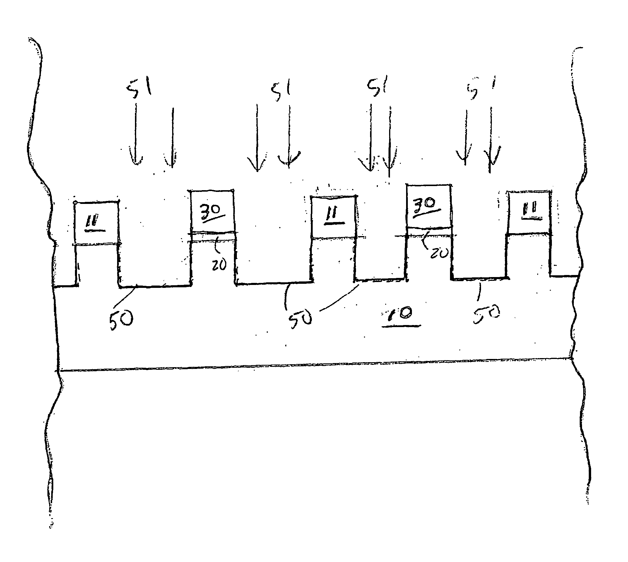
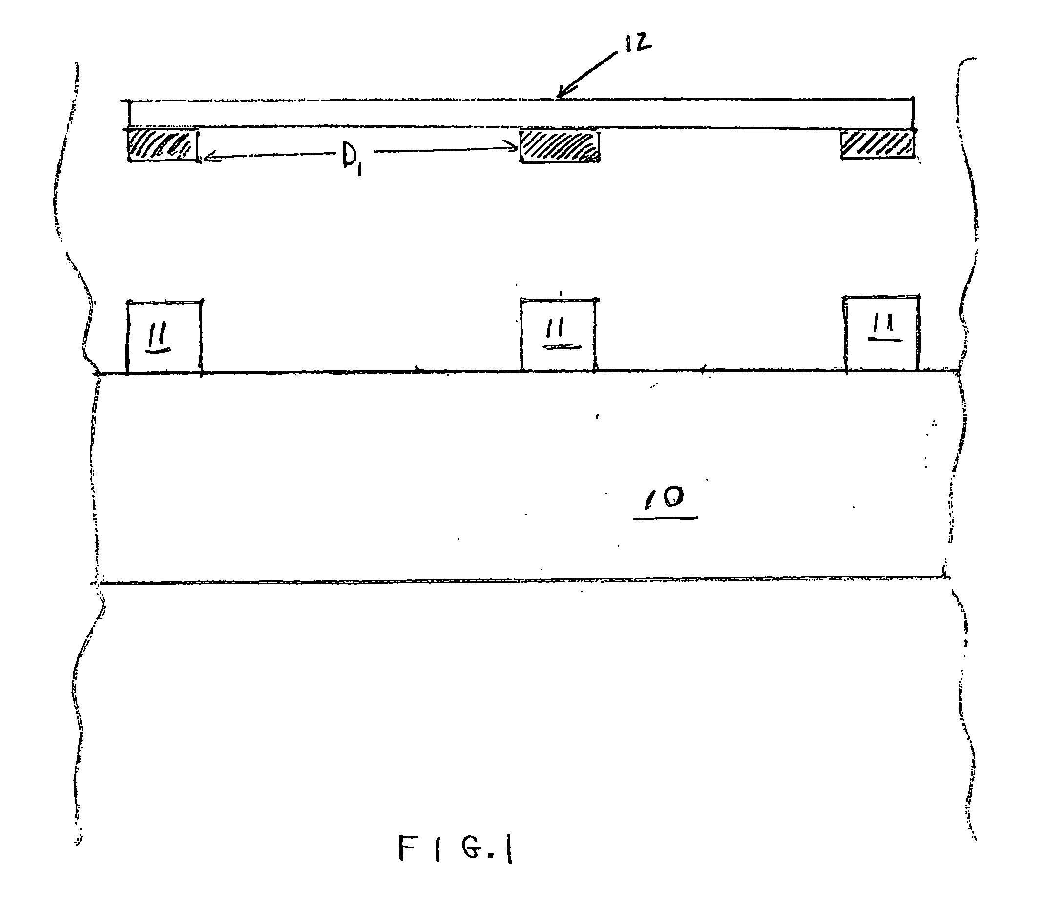
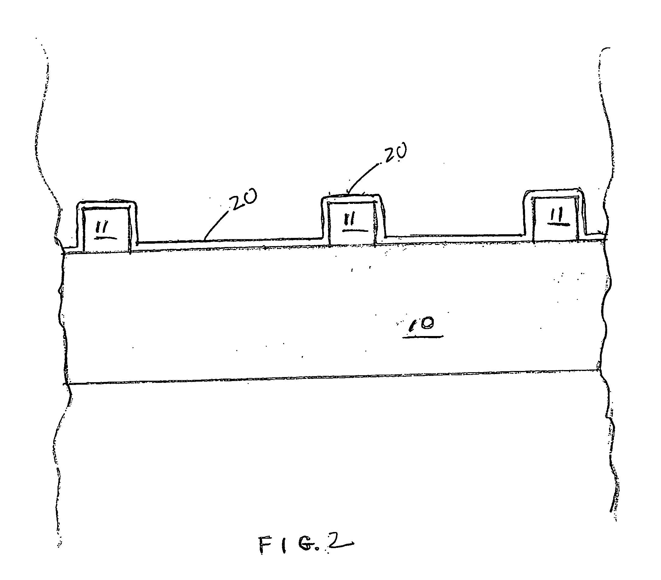
[0014]The present invention addresses and solves problems attendant upon fabricating semiconductor devices comprising features with accurately formed dimensions in the decananometer range, e.g., with device features of 45 nm and under, features used for 65 nm technology or beyond, such as len than 90 nm half pitch, line end shortening, line-to-printing, and T-shape printing. These problems stem from dimensional restrictions imposed by the chemical and optical limits of conventional lithography systems and distortions of feature shape, such as corner rounding when forming negative features in a target substrate. The present invention provides methodology enabling the formation of various types of semiconductors having such ultrafine features with high dimensional accuracy, in an efficient manner and in a single tool, thereby reducing manufacturing costs and increasing manufacturing throughput.

[0015]In accordance with embodiments of the present invention, a double exposure technique i...


PUM

PropertyMeasurementUnit
distanceaaaaaaaaaa
dielectric constantaaaaaaaaaa
antireflectiveaaaaaaaaaa

Abstract

Ultrafine patterns with dimensions smaller than the chemical and optical limits of lithography are formed by superimposing two photoresist patterns using a double exposure technique. Embodiments include forming a first resist pattern over a target layer to be patterned, forming a protective cover layer over the first resist pattern, forming a second resist pattern on the cover layer superimposed over the first resist pattern while the cover layer protects the first resist pattern, selectively etching the cover layer with high selectivity with respect to the first and second resist patterns leaving an ultrafine target pattern defined by the first and second resist patterns, and etching the underlying target layer using the superimposed first and second resist patterns as a mask.

Description

FIELD OF THE INVENTION[0001]The present invention relates to the fabrication of semiconductor devices having closely spaced apart transistors and high speed integrated circuits with design features in the deep sub-micron range.BACKGROUND ART[0002]As the dimensions of semiconductor device features continue to shrink into the deep sub-micron range, as in the decananometer range, it becomes increasingly more difficult to form the features with high dimensional accuracy. The minimum size of a feature depends upon the chemical and optical limits of a particular lithography system, and the tolerance for distortions of the shape, such as corner rounding when forming negative features in a target layer or substrate.[0003]Accordingly, a need exists for methodology enabling the fabrication of semiconductor devices having accurately formed features in the deep sub-micron range, such as features of 45 nm and under, in addition to features used for 65 nm technology and beyond, e.g., less than 90...

Claims


Application Information

Patent Timeline
Patent Type & Authority Applications(United States)
IPC IPC(8): G03F7/26
CPCG03F7/70466G03F7/0035G03F1/70
Inventor KIM, RYOUNG-HANKYE, JONG-WOOK
Owner ADVANCED MICRO DEVICES INC
Why Eureka
Try Eureka