Selective Encapsulation of Electronic Components

a technology of electronic components and encapsulation, which is applied in the direction of printed circuit aspects, sustainable manufacturing/processing, final product manufacturing, etc., can solve the problems of difficult to precisely control the perimeter within which the resin will reside, the relatively uncontrolled process, and the inability to provide a uniform encapsulation of the component, so as to reduce the heat exposure of the components, reduce the time of process, and reduce the requirement of materials

Inactive Publication Date: 2007-12-20
LHV POWER
View PDF3 Cites 24 Cited by
  • Summary
  • Abstract
  • Description
  • Claims
  • Application Information

AI Technical Summary

Benefits of technology

[0016] It is an advantage of the present invention to provide a simplified method for the encapsulation of electronic components, wherein process times are reduced, materials requirements are decreased, and heat exposure of the components is lowered in comparison with the prior art.
[0017] It is another advantage of the present invention to provide a method for the selective encapsulation of electronic components that enables both the precise positioning of the resin over the areas to be encapsulated and the encapsulations of different components with resin layers of different thicknesses.
[0018] Still another advantage of the present invention is to provide a method that enables designers and manufacturers of PCBs to reduce spacing between components and to increase component density on the boards.
[0019] These and other advantages of the present invention will become apparent from a reading of the following description, and may be realized by means of the instrumentalities and combinations particularly pointed out in the appended claims.

Problems solved by technology

It is evident, however, that this process is relatively uncontrolled.
The encapsulating resin creates a mound over the target component and generally does not provide a uniform encapsulation of the component.
It is also very difficult to control precisely the perimeter within which the resin will reside.
Thus, while the dam & fill process provides a more accurate resin placement than the glob top process, it also requires extended heat application to the board, which increases process costs and which may damage the electronic components.
Further, the low viscosity of the heated fill resin may generate resin runoffs and hinder a precise positioning of the resin within narrowly defined areas of the board or on certain portions only of the components, making the dam & fill process suitable only for the encapsulation of extended portions of a PCB, rather than for the selective encapsulation of portions of individual components or of narrowly defined areas of the PCB.

Method used


Image

  • Selective Encapsulation of Electronic Components
  • Selective Encapsulation of Electronic Components
  • Selective Encapsulation of Electronic Components

Examples


first embodiment

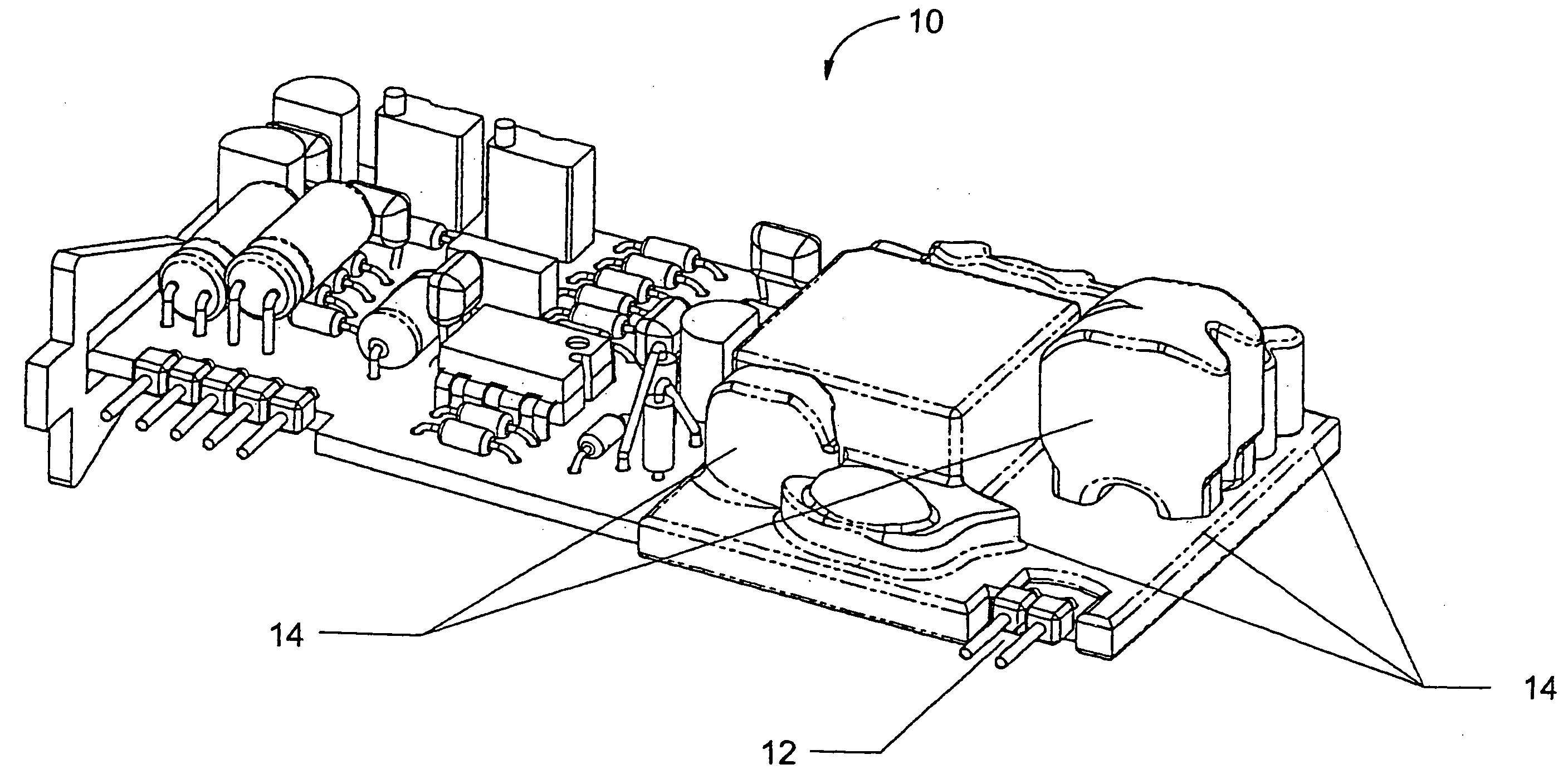
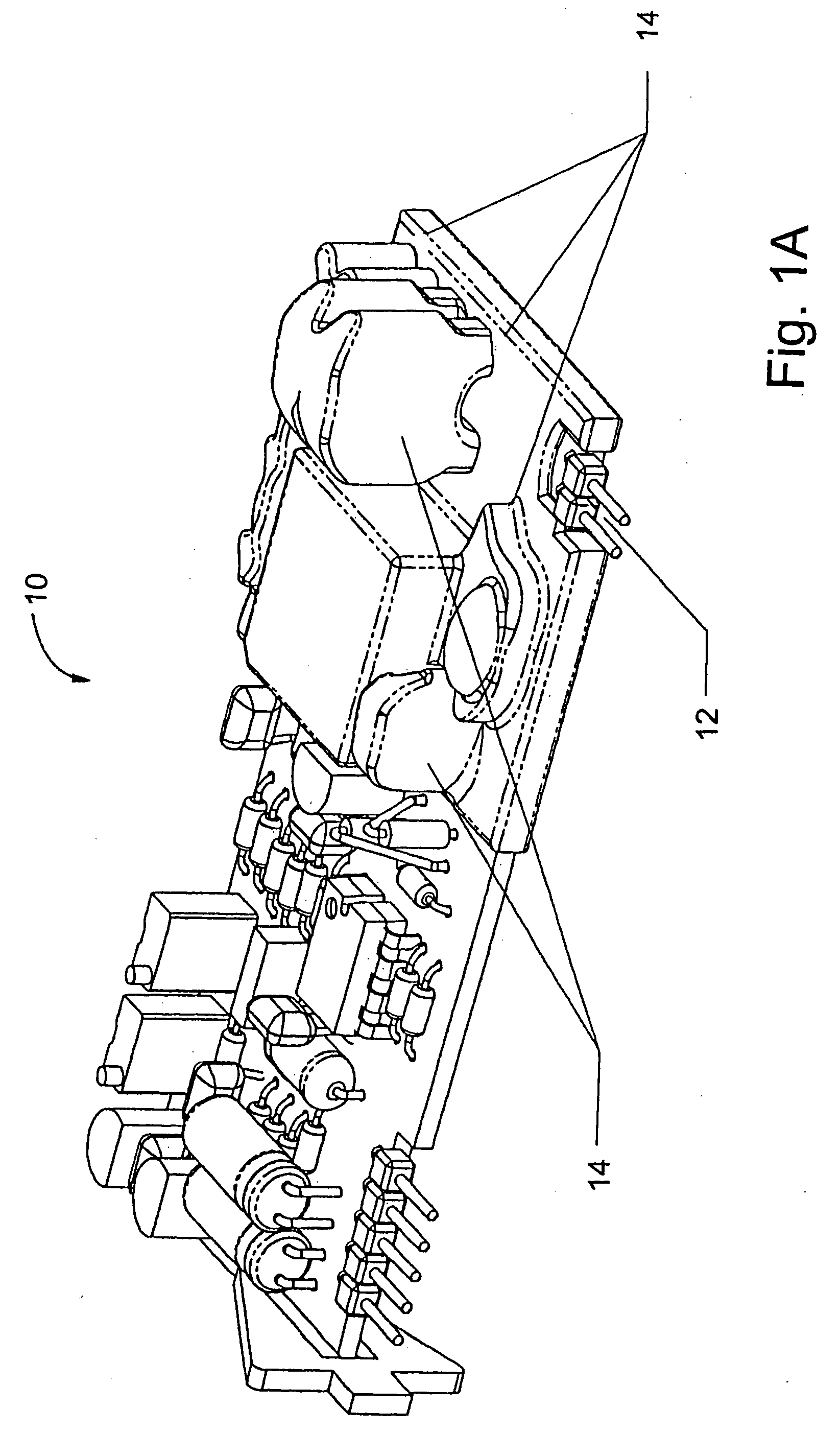
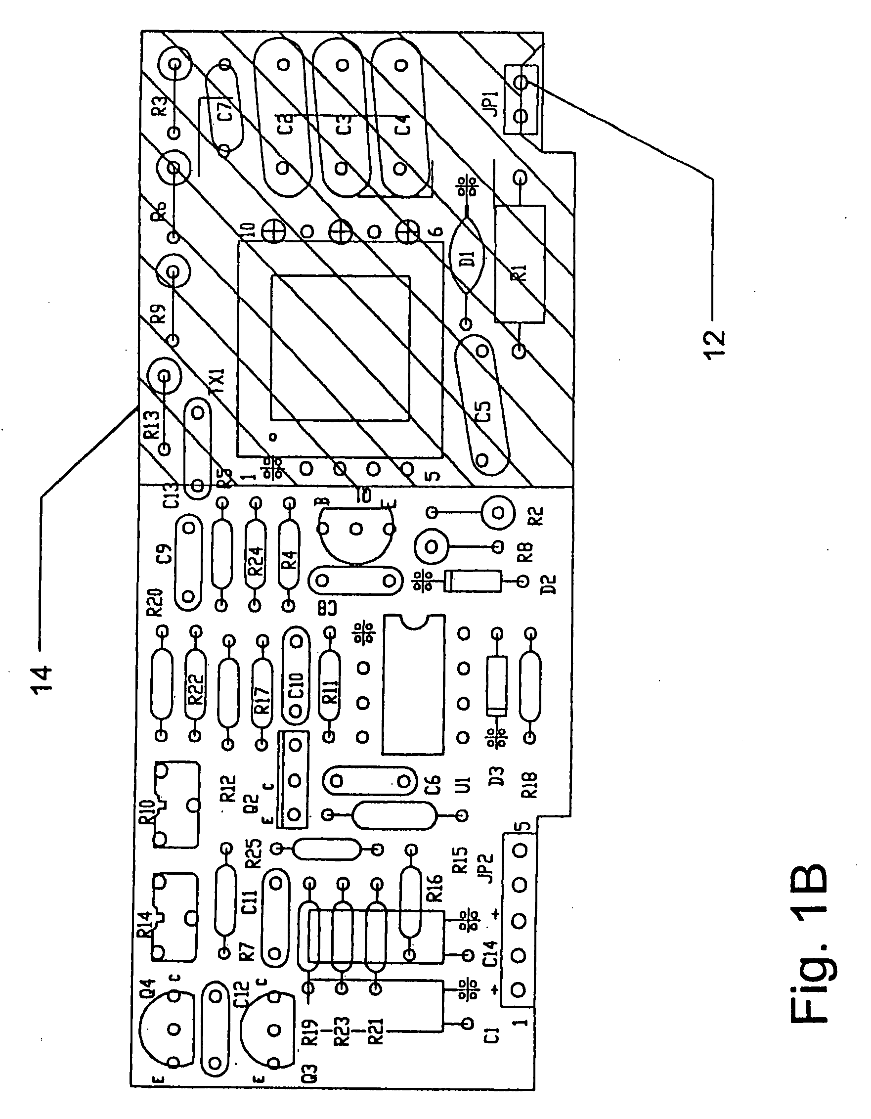
[0033] The steps comprised in the invention are summarized in FIG. 2. In the first step, a PCB is delivered to an encapsulating nest in a room temperature environment, preferably with an automated delivery line.

[0034] In the second step, the target areas of the board are surrounded by a dam, which may encircle entire portions of the board, individual components on the board, or even portions of individual components, if it is desired to leave portions of certain components non-encapsulated after processing.

[0035] The dam comprises a resin (typically, an epoxy resin) of a thixotropy such to enable an easy yet accurate resin placement, and to maintain the resin in place during processing, thereby avoiding resin run-offs. The dam resin may be a system of two chemical components that are mixed in situ, wherein one component is a base resin and the second component is a curing agent, or is preferably a pre-mixed resin delivered as a mono-component system. In either case, the curing agen...

second embodiment

[0048] In the second embodiment, a substrate 18 is delivered to an encapsulating nest at room temperature, and a resin bead 20, such as an epoxy bead, is laid in a position preferably transverse in relation to a target electronic component 22, for instance, in a direction that is perpendicular to component 22 and preferably bisects a line drawn between the PCB contact pads or through-holes. One skilled in the art will recognize that the size of bead 20 will be determined according to the size of the component to be placed.

[0049] The resin beads not only act as primary dielectric barriers, but also aid component retention during assembly. As an additional benefit, the beads further reduce potential entrapments of gases within the fill resin.

[0050] After bead deposition and component placement, the components are soldered, and the components are encapsulated as in the first embodiment.

[0051] Turning now to FIGS. 4, 5A, and 5B, there is shown the practice of the second embodiment of ...


PUM

PropertyMeasurementUnit
voltageaaaaaaaaaa
temperatureaaaaaaaaaa
electrical insulationaaaaaaaaaa

Abstract

A method for the selective encapsulation of electronic components on a printed circuit board comprising, in one embodiment, the steps of delivering the printed circuit board to an encapsulating nest at room temperature; damming the target areas with a dam resin having a latent curing agent and deposited in the shape of walls of predetermined heights, according to the desired fill heights; dispensing a fill resin to fill the dammed areas; and curing the dam and fill resins for a suitable amount of time. In a different embodiment, the invention comprises the additional steps of laying resin beads, each in a position corresponding to the footprint of each target component; and of positioning the target components over the beads and soldering the components.

Description

FIELD OF THE INVENTION [0001] The present invention relates to a method for the selective encapsulation of electronic components. More particularly, the present invention relates to a method for the selective encapsulation of certain electronic components on a printed circuit board or portions thereof, within predefined perimeters and with resin layers of predetermined thicknesses. BACKGROUND OF THE INVENTION [0002] Electronic components on printed circuit boards often require protection from a variety of threats. For instance, designers and manufacturers often need to protect electronic components from adverse physical and environmental impacts, such as shock, moisture, contamination, or abuse; from voltage differentials with neighboring components; or from “reverse engineering” by competitors seeking to copy proprietary designs. [0003] To protect electronic components, some manufacturers employ an over-molding process that encases the electronic components in a plastic shell. Othe...

Claims


Application Information

Patent Timeline
Patent Type & Authority Applications(United States)
IPC IPC(8): H05K3/30
CPCH01L21/56H05K3/284H05K3/305H05K2201/0187H05K2201/09909Y10T29/49146H05K2203/1476H01L2924/0002H05K2203/0126Y10T29/49171H01L2924/00Y02P70/50
Inventor WING, KENNETH E.CARROLL, SCOTT T.
Owner LHV POWER
Why Eureka
Try Eureka