

Substrate of liquid crystal device and method for manufacturing the same
a liquid crystal display and substrate technology, applied in semiconductor devices, semiconductor/solid-state device details, instruments, etc., can solve the problems of reducing the signal-transmitting rate and the fact that the rc delay in the signal-transmitting rate of metal conductive lines is in fact more critical, so as to achieve low electric resistance and high image quality
- Summary
- Abstract
- Description
- Claims
- Application Information
AI Technical Summary
Benefits of technology
Problems solved by technology
Method used
Image


Examples
embodiment 2
[0049]The method for manufacturing a substrate of the TFT LCD device in the present embodiment is the same as illustrated in the embodiment 1 except a barrier layer is formed on the surface of the TFT source and drain, and the buffer layer is made of silicon nitride (SiN). Other conditions and steps in the manufacture are the same as in the embodiment 1.
[0050]FIGS. 2 (a) to FIG. 2 (g) are flowcharts of the preferable embodiment for manufacturing the substrate of the LCD device in the present invention.
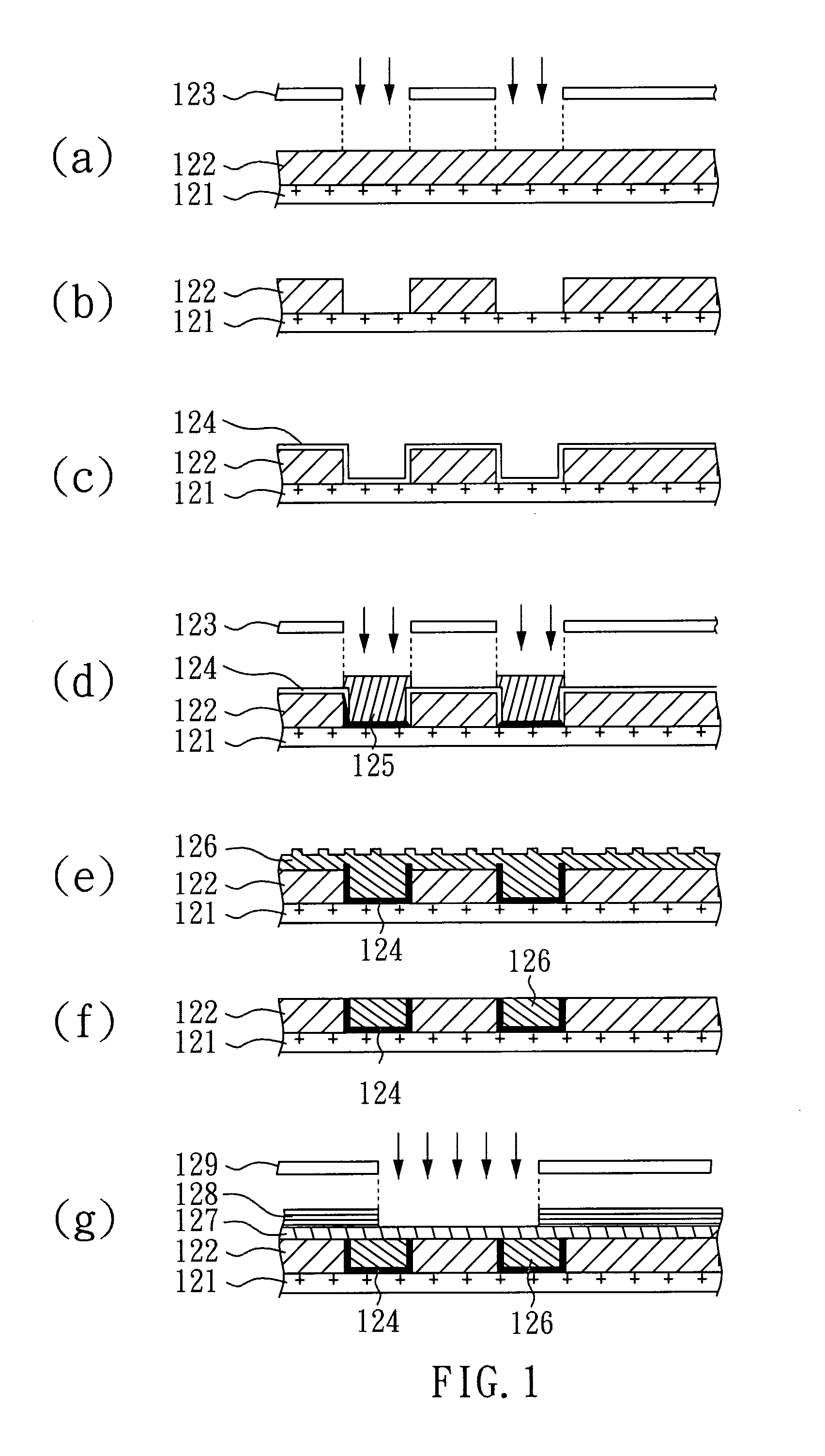
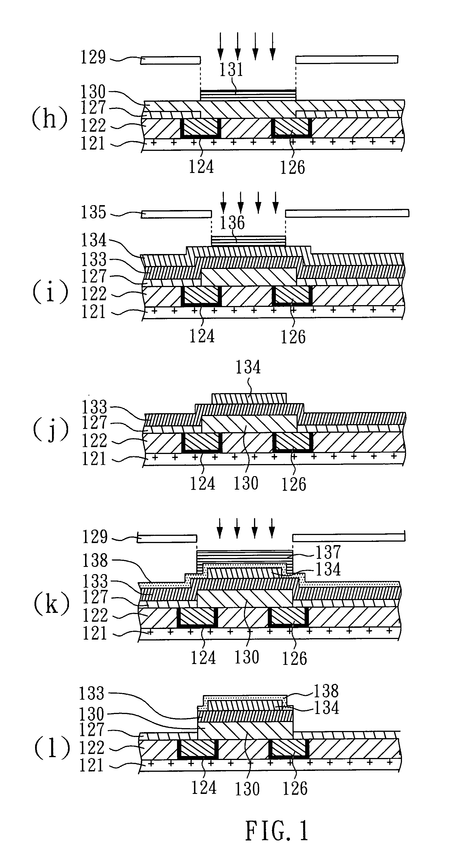
[0051]FIG. 2 (a) shows that a substrate 121 is provided. A first metal layer 126 for the source and drain is formed according to the procedures shown in FIG. 1 (a) to FIG. 1 (f) in the embodiment 1.
[0052]Subsequently, by way of plasma enhanced chemical vapor deposition, the first metal layer is annealed in the condition of filled with SiH4 gas at 350° C. On the surface of the first metal layer 126 made of copper, a copper silicon compound is formed to be a barrier layer 250 on the sour...
embodiment 3
[0053]The method for manufacturing a substrate of the TFT LCD device in the present embodiment is the same as illustration in the embodiment 1 and 2, except that the semi-conductive layer made of polycrystalline silicon is implanted ionic dopants in the polycrystalline silicon semi-conductive layer. Other conditions and steps in the manufacture are the same as in the embodiments 1 and 2.
[0054]FIG. 3 (a) to FIG. 3 (h) are flowcharts of the preferable embodiment for manufacturing the substrate of the LCD device in the present invention.
[0055]As shown in FIG. 3 (a), a first metal layer 126 forming a source / drain on a substrate 121 is provided. The manufacturing steps of the first metal layer 126 are according to the flowchart shown in FIG. 1 (a) to FIG. 1 (f) of the embodiment 1. As illustrated in the embodiment 2 and shown in FIG. 2 (a), on the surface of the first metal layer 126, a copper silicon compound is formed to be a barrier layer 250. Subsequently, a patterned transparent con...
embodiment 4
[0060]The method for manufacturing a substrate of the TFT LCD device in the present embodiment is the same as illustration in the embodiment 1, except that ionic dopants are implanted into the semi-conductive layer made of polycrystalline silicon. Other conditions and steps in the manufacture are the same as in the embodiment 1.
[0061]FIG. 4 (a) to FIG. 4 (h) are flowcharts of the preferred embodiment for manufacturing the substrate of the LCD device in the present invention. As shown in FIG. 4 (a), a substrate 121, on which a first metal layer 126 having the source / drain is formed, is provided. The manufacturing method of the substrate 121 is according to the flowchart of the embodiment 1 shown in FIG. 1 (a) to FIG. 1 (f). Subsequently, a patterned transparent conductive layer 127 is formed over the substrate 121.
[0062]An amorphous silicon layer made of SiN 430a and an a-Si:H amorphous silicon layer 430b, respectively covering the first insulation layer 122 and the transparent condu...
PUM
| Property | Measurement | Unit |
|---|---|---|
| semi-conductive | aaaaa | aaaaa |
| P-type semi-conductive | aaaaa | aaaaa |
| transparent | aaaaa | aaaaa |
Abstract
Description
Claims
Application Information