Crystalline Silicon Wafer, Crystalline Silicon Solar Cell, Method of Manufacturing Crystalline Silicon Wafer, and Method of Manufacturing Crystalline Silicon Solar Cell

a technology of crystalline silicon and solar cells, which is applied in the direction of semiconductor/solid-state device manufacturing, electrical apparatus, and semiconductor devices. it can solve the problems of high probability of adverse effects on subsequent steps, damage to the slicing step surface, and high probability of impurities causing adverse effects on the subsequent steps, so as to reduce solar light reflection loss

Inactive Publication Date: 2008-01-03
SHARP KK
View PDF1 Cites 34 Cited by
  • Summary
  • Abstract
  • Description
  • Claims
  • Application Information

AI Technical Summary

Benefits of technology

[0029] According to the present invention, it is possible to provide a crystalline silicon wafer, a crystalline silicon solar cell, a method of manufacturing the crystalline silicon wafer, and a method of manufacturing the crystalline silicon solar cell, which can reduce solar light reflection loss at a surface.

Problems solved by technology

Although not all these machining processes are performed, the block producing step and the slicing step are essential, and hence a surface of the wafer subjected to the slicing step has a damaged layer, namely, a work-affected layer formed thereat.
Additionally, the work-affected layer includes, as residues, abrasive grains and a lubricant used in processing, which have a high probability of causing adverse effects on subsequent steps as impurities.
However, a film thickness thereof inevitably limits a wavelength range in which reflection is reduced.
However, increase in production steps inevitably raises manufacturing cost.

Method used


Image

  • Crystalline Silicon Wafer, Crystalline Silicon Solar Cell, Method of Manufacturing Crystalline Silicon Wafer, and Method of Manufacturing Crystalline Silicon Solar Cell
  • Crystalline Silicon Wafer, Crystalline Silicon Solar Cell, Method of Manufacturing Crystalline Silicon Wafer, and Method of Manufacturing Crystalline Silicon Solar Cell
  • Crystalline Silicon Wafer, Crystalline Silicon Solar Cell, Method of Manufacturing Crystalline Silicon Wafer, and Method of Manufacturing Crystalline Silicon Solar Cell

Examples


example

Example 1

[0072] Initially, a polycrystalline silicon ingot was formed by a cast method. In the cast method, a polycrystalline silicon ingot was formed by slowly cooling silicon melted in a casting mold (cast) at a temperature of approximately 1400° C. to 1500° C., which temperature is equal to or higher than a melting point of silicon, and solidifying the same.

[0073] The polycrystalline silicon ingot was removed from the casting mold, and processed with a band saw into a rectangular parallelepiped block having a square base with a side of 125 mm and a thickness of approximately 20 cm. The polycrystalline silicon ingot subjected to the block producing process as described above was sliced by means of a wire saw provided with a multiwire and abrasive grains made of SiC (silicon carbide), so that there were obtained silicon wafers each having a thickness of 300 μm. At that time, each of the abrasive grains had a grain size of not less than 10 μm and not more than 40 μm.

[0074] The si...

example 2

[0080] A crystalline silicon solar cell was fabricated with the use of the crystalline silicon wafer in Example 1. For comparison, a crystalline silicon solar cell was fabricated with the use of the crystalline silicon wafer in Comparative Example 1. At that time, these crystalline silicon wafers had a p-conductivity type, and had a specific resistance of approximately 1 Ω·cm.

[0081] Next, a diffusing agent containing phosphorus was applied to the surfaces of the crystalline silicon wafers, which surfaces were to serve as light-receptive surfaces, and the crystalline silicon wafers were heated to 900° C. to thermally diffuse phosphorus in the light-receptive surfaces of these crystalline silicon wafers, so that n-type diffusion layers having a sheet resistance value of approximately 50Ω were formed.

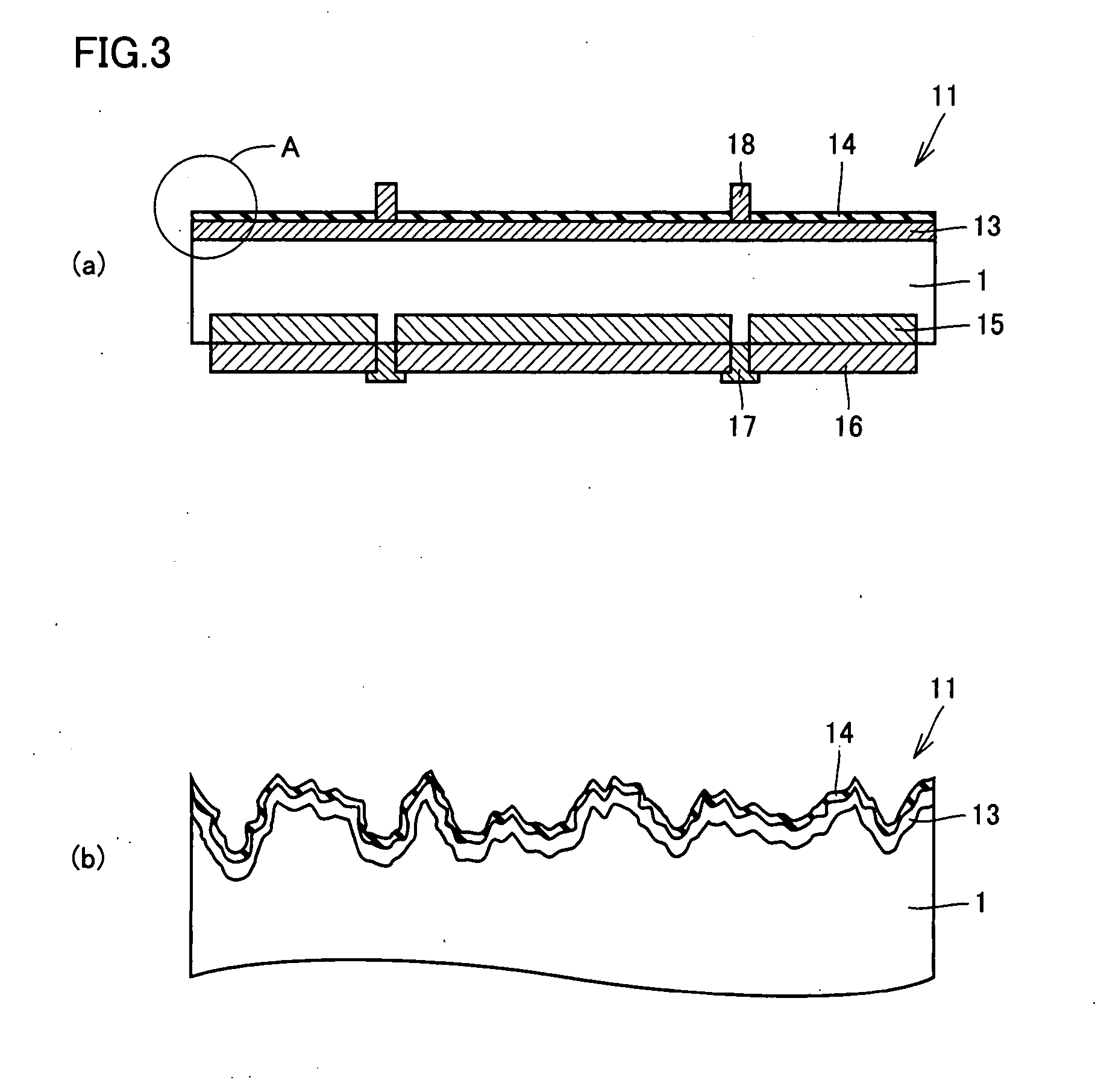
[0082] Next, on each of the n-type diffusion layers, there was deposited a silicon nitride film having a thickness of approximately 70 nm by a plasma CVD method, to serve as an antirefle...


PUM

PropertyMeasurementUnit
heightaaaaaaaaaa
heightaaaaaaaaaa
widthaaaaaaaaaa

Abstract

There is disclosed a crystalline silicon wafer (1) having irregularities formed at its surface. The irregularities include first irregularities (2) and second irregularities (3) smaller than the first irregularities (2). There are also disclosed a crystalline silicon wafer solar cell (11) using the crystalline silicon wafer (1), a method of manufacturing the crystalline silicon wafer (1), and a method of manufacturing the crystalline silicon wafer solar cell (11).

Description

TECHNICAL FIELD [0001] The present invention relates to a crystalline silicon wafer, a crystalline silicon solar cell, a method of manufacturing the crystalline silicon wafer, and a method of manufacturing the crystalline silicon solar cell. BACKGROUND ART [0002] A crystalline silicon wafer, which is most frequently used for a semiconductor device, is obtained from a monocrystalline silicon ingot made by a Czochralski (CZ) method or a polycrystalline silicon ingot made by a cast method, subjected to machining processes such as a block producing step, a profile grinding step, a slicing step, a lapping step, and others. Although not all these machining processes are performed, the block producing step and the slicing step are essential, and hence a surface of the wafer subjected to the slicing step has a damaged layer, namely, a work-affected layer formed thereat. [0003] The machining processes and work-affected layer described above are explained in detail in Non-Patent Document 1 (F...

Claims


Application Information

Patent Timeline
Patent Type & Authority Applications(United States)
IPC IPC(8): H01L31/00H01L21/02
CPCH01L31/035281H01L31/02363Y02E10/50H01L31/03529
Inventor OTAKE, YASUTOSHIHAGINO, MASATO
Owner SHARP KK
Why Eureka
Try Eureka