Organic electroluminescence device
a technology of electroluminescence device and organic compound layer, which is applied in the direction of discharge tube/lamp details, luminescent screen of discharge tube, organic semiconductor device, etc., can solve the problems of easy degradation of characteristic characteristics of organic el device, peeling of organic compound layer and electrode layer, dark spots, etc., and achieves easy optical adjustment
- Summary
- Abstract
- Description
- Claims
- Application Information
AI Technical Summary
Benefits of technology
Problems solved by technology
Method used
Image

Examples
first embodiment
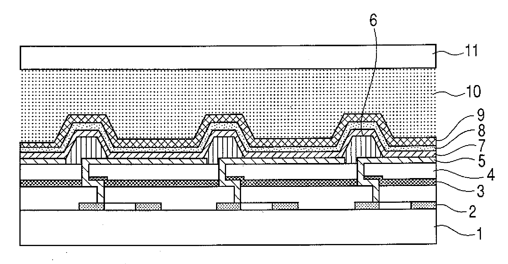
[0017]FIG. 1 is a schematic view illustrating a part of cross section of a top emission type organic EL device of the present invention.
[0018]First, reference numerals in the drawings are described.
[0019]There are provided a glass substrate 1, a TFT (thin-film transistor) 2, an insulating film 3, an organic planarizing film 4, an opaque electrode 5, a device isolation film 6, an organic compound layer 7, a transparent electrode 8, a passivation layer 9, a filling layer 10, a cover glass 11 and a sealing can 12.
[0020]On the glass substrate (substrate) 1, the TFT 2, the insulating film 3 and the organic planarizing film 4 are formed by stacking in this order, and thereon a Cr electrode which is an opaque electrode 5 as pixel (device) unit is formed. The surrounding of each pixel is covered with a device isolation film 6 made of polyimide. Above this substrate, an organic compound layer 7 having a hole transport layer, a light-emitting layer, an electron transport layer and an electron...
second embodiment
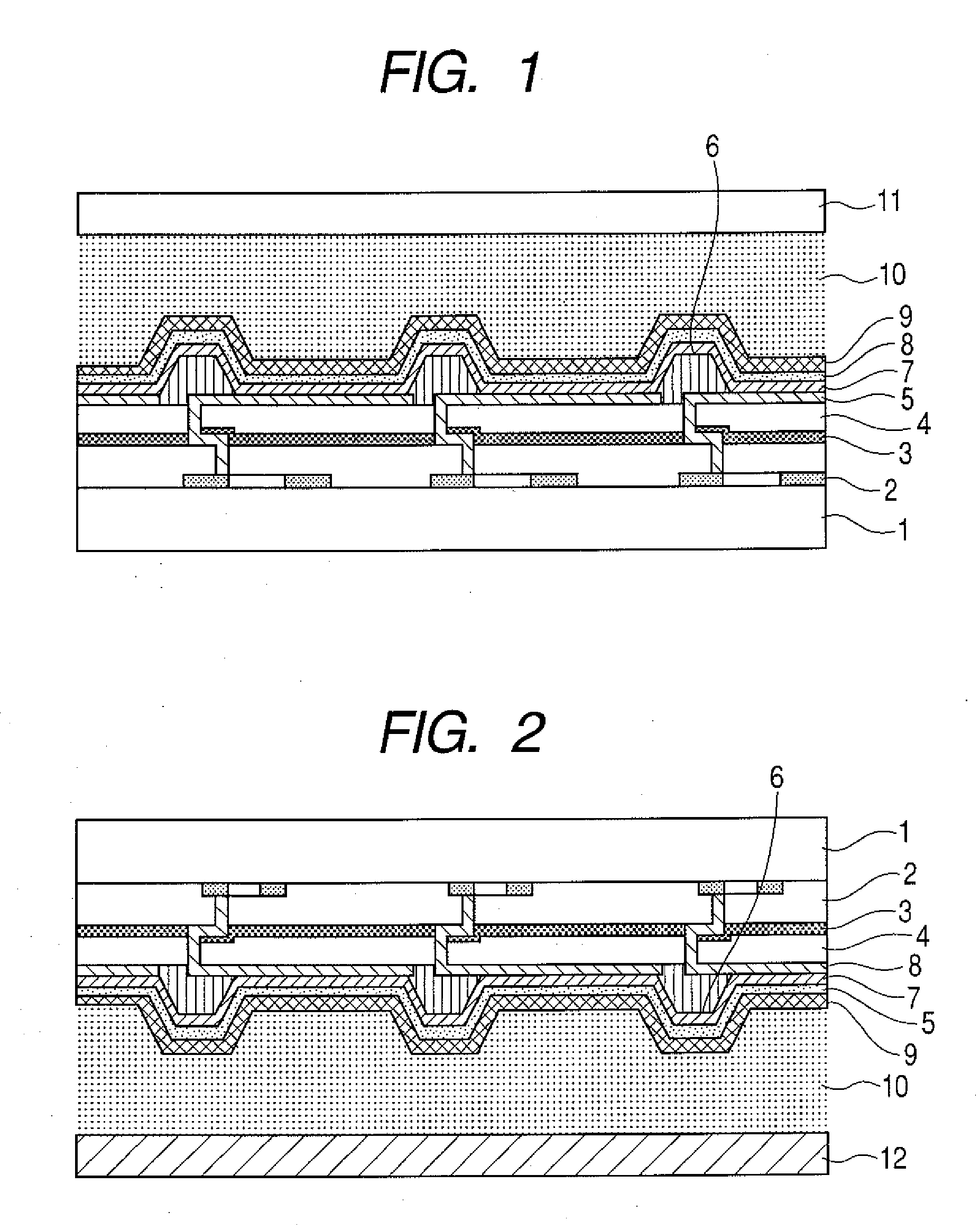
[0032]FIG. 2 is a schematic view illustrating a part of cross section of a bottom emission type organic EL device of the present invention.
[0033]In the organic EL device shown in FIG. 2, a TFT 2, an insulating film 3 and an organic planarizing film 4 are formed in this order under a glass substrate 1, and on the organic planarizing film, an ITO electrode as a transparent electrode (first electrode) 8 for pixel unit is formed. The surrounding of each pixel is covered with a device isolation film 6 made of polyimide. Below this substrate, an organic compound layer 7 having a hole transport layer, a light-emitting layer, an electron transport layer and an electron injection layer in this order is formed. Under the organic compound layer, an opaque electrode (second electrode) 5 and a passivation layer 9 are formed in this order. Then, the transparent electrode 8 except a lead-out electrode, the organic compound layer 7, the device isolation film 6 and the organic planarizing film 4 are...
example 1
[0039]The inside of a 500 ml-flask equipped with a nitrogen inlet tube and a cooling tube is replaced with a nitrogen gas. In the flask, placed are 100 g of styrene monomer (manufactured by Kishida Chemical Co., Ltd.); 100 g of butyl methacrylate (manufactured by Kishida Chemical Co., Ltd.); 200 ml of dehydrated dimethylformamide (manufactured by Kishida Chemical Co., Ltd.); and 20 g of azobisisobutyronitrile (manufactured by Kishida Chemical Co., Ltd.), from all of which dehydration treatment and removal of polymerization inhibitors have been conducted. After the inside of the flask is replacement with a nitrogen gas, the obtained mixture is heated to 80° C. and stirred for 5 hours. The resultant liquid is poured into a beaker containing 1 L of methanol for reprecipitation. The obtained solid product is cleaned with methanol, and heated and dried under vacuum to obtain 145 g of poly(styrene-butyl methacrylate) as a polymer.
[0040]100 g of the obtained polymer is heated and dried und...
PUM
| Property | Measurement | Unit |
|---|---|---|
| Refractive index | aaaaa | aaaaa |
| Optical properties | aaaaa | aaaaa |
Abstract
Description
Claims
Application Information