

Light emitting device containing phosphorescent complex
- Summary
- Abstract
- Description
- Claims
- Application Information
AI Technical Summary
Benefits of technology
Problems solved by technology
Method used
Image

Examples
examples
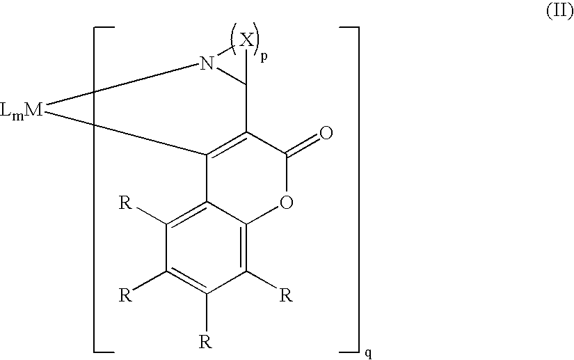
[0311]Preparation of 2H-1-Benzopyran-2-one, 3-(2-pyridinyl (3-(2-pydinyl)coumarin or pcm): o-hydoxycarbonylbenzene (40 mmol) and 2-pyridylacetonitrile (40 mmol) were added to an aqueous solution of NaOH (0.05 N, 200 ml). The mixture was vigorously stirred at 90° C. for 3.5 hours. After cooling the solid was filtered, washed with cold water and dried. The crude compound was purified by crystallization from ethanol. yield: 92%. MS: m / z calcd 223; found 224 [M+1].
[0312]Synthesis of Ir(3-pyridylcoumarin)2(acac) (Ir(pcm)2acac) (CMPD-1): Cyclometalated Ir(III) μ-chloro-bridged dimer of (pcm)2Ir (μ-Cl)2Ir(pcm)2 was synthesized according to the Nonoyama route, by refluxing IrCl3.nH2O with 2-2.5 equiv of 3-pyridylcoumarin in a 3:1 mixture of 2-ethoxyethanol and water. The chloro-bridged dimer complex (0.08 mmol), 0.2 mmol of acetyl acetone, and 85-90 mg of sodium carbonate were heated to reflux in dichloroethane under an inert atmosphere for 12-15 hours. After cooling, the mixture was extrac...
examples 1-1 through 1-6
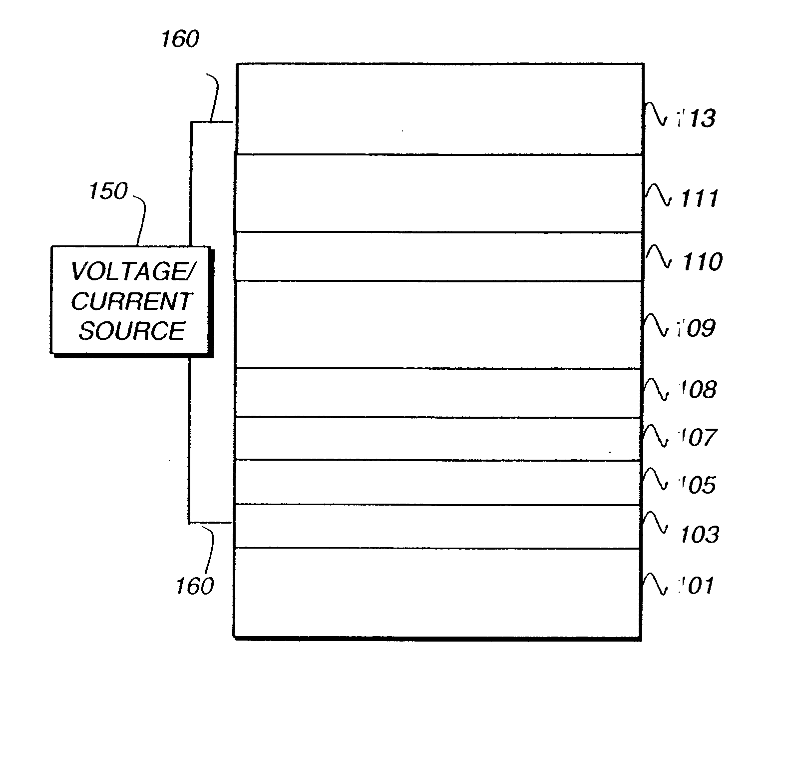
[0316]EL devices (Examples 1-1 through 1-6) satisfying the requirements of the invention were constructed in the following manner:[0317]1. A glass substrate, coated with an approximately 25 nm layer of indium-tin oxide (ITO) as the anode, was sequentially ultrasonicated in a commercial detergent, rinsed in deionized water, degreased in toluene vapor and exposed to an oxygen plasma for about 1 minute.[0318]2. Over the ITO a 1 nm fluorocarbon (CFx) hole injecting layer (HIL) was deposited by plasma-assisted deposition of CHF3 as described in U.S. Pat. No. 6,208,075.[0319]3. Next, a hole transporting layer (HTL) of N,N′-di-1-naphthyl-N,N′-diphenyl-4,4′-diaminobiphenyl (NPB) was vacuum deposited to a thickness of 75 nm for Examples 1-1 through 1-4 and 95 nm for Examples 1-5 and 1-6.[0320]4. A 40 nm light emitting layer (LEL) consisting of a mixture of CBP, and INV-1 as a phosphorescent emitter was then vacuum deposited onto the hole transporting layer. The weight % of the phosphorescent...
examples 2-1 through 2-2
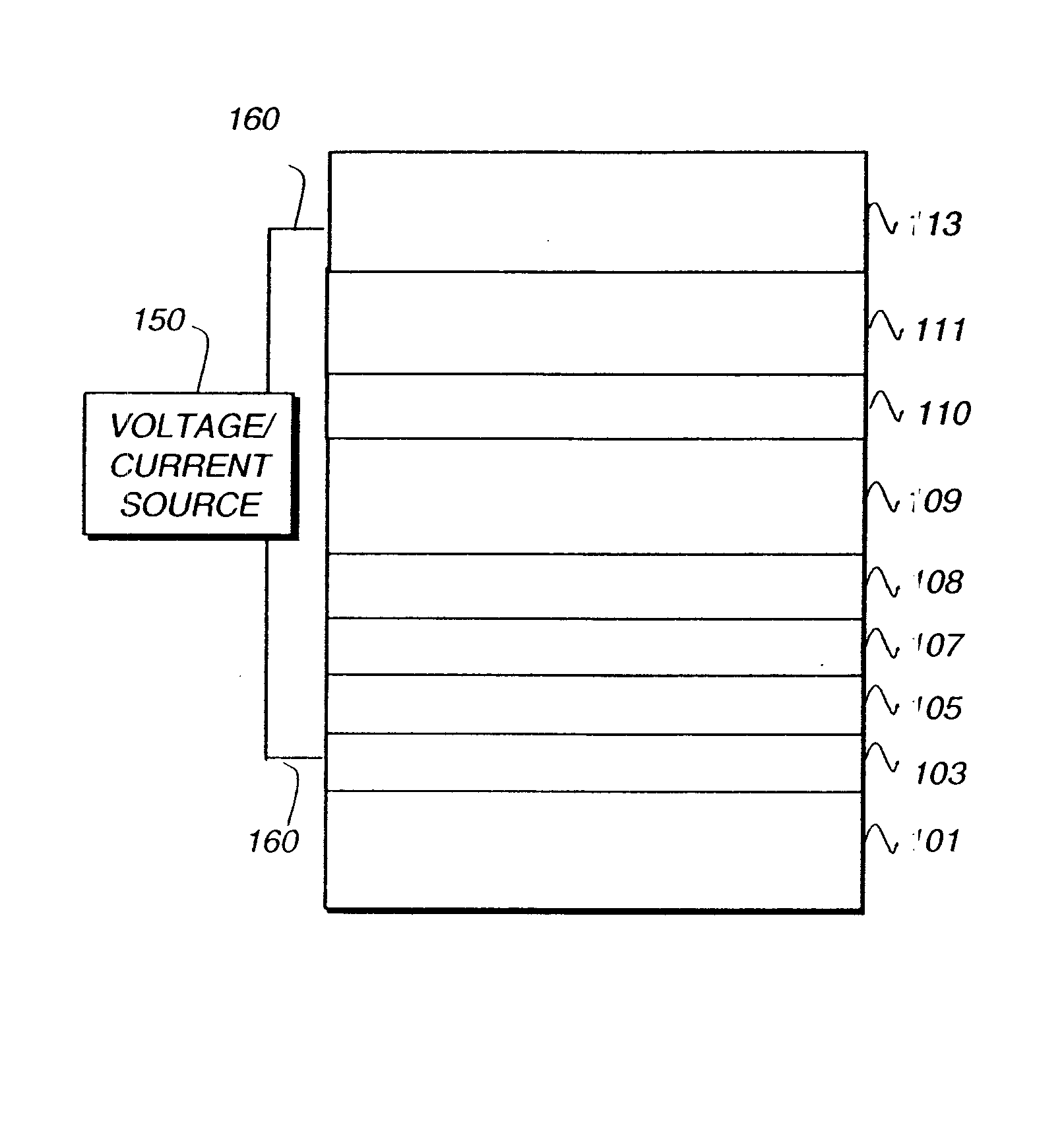
[0326]EL devices (Example 2-1 and 2-2) satisfying the requirements of the invention were constructed in the following manner:[0327]1. A glass substrate, coated with an approximately 25 nm layer of indium-tin oxide (ITO) as the anode, was sequentially ultrasonicated in a commercial detergent, rinsed in deionized water, degreased in toluene vapor and exposed to an oxygen plasma for about 1 minute.[0328]2. Over the ITO a 1 nm fluorocarbon (CFx) hole injecting layer (HIL) was deposited by plasma-assisted deposition of CHF3 as described in U.S. Pat. No. 6,208,075.[0329]3. Next, a hole transporting layer (HTL) of N,N′-di-1-naphthyl-N,N′-diphenyl-4,4′-diaminobiphenyl (NPB) was vacuum deposited to a thickness of 95 nm.[0330]4. A exciton blocking layer (EBL) of TCTA was vacuum deposited over the HTL to a thickness of 10 nm.[0331]5. A 35 nm light emitting layer (LEL) consisting of a mixture of TPBI, TCTA, and INV-1 as a phosphorescent emitter was then vacuum deposited onto the exciton blockin...
PUM
| Property | Measurement | Unit |
|---|---|---|
| Fraction | aaaaa | aaaaa |
| Fraction | aaaaa | aaaaa |
| Fraction | aaaaa | aaaaa |
Abstract
Description
Claims
Application Information