
Germanium compound, semiconductor device fabricated using the same, and methods of forming the same

a technology of germanium compound and semiconductor device, applied in germanium organic compound, organic chemistry, instruments, etc., can solve the problems of nonvolatile memory device retaining stored data, reducing the size of phase change material pattern, and losing data stored within volatile memory devi

Active Publication Date: 2008-02-14
SAMSUNG ELECTRONICS CO LTD +1
View PDF11 Cites 37 Cited by
  • Summary
  • Abstract
  • Description
  • Claims
  • Application Information

AI Technical Summary

Benefits of technology

[0011] Embodiments exemplarily described herein can be generally characterized as being directed to a germanium compound useful in forming a substantially uniform layer and a method of forming the same. Also, embodiments exemplarily described herein can be generally characterized as being directed to semiconductor devices and methods of forming the same using the germanium compound.
[0012] One embodiment exemplarily described herein can be characterized as a germanium compound having a chemical formula GeR1xR2y. “R1” is an alkyl group, and “R2” is one of hydrogen, an amino group, an allyl group and a vinyl group. “x” is greater than zero and less than 4, and sum of “x” and “y” equal to 4. In one embodiment, “R1” may comprise iso-propyl. In another embodiment, the amino group may comprise NR3R4, and each of “R3” and “R4” may be an alkyl group. In yet another embodiment, “R3” may be one of methyl, ethyl, iso-propyl and tert-butyl, and “R4” may be one of methyl, ethyl, iso-propyl and tert-butyl.
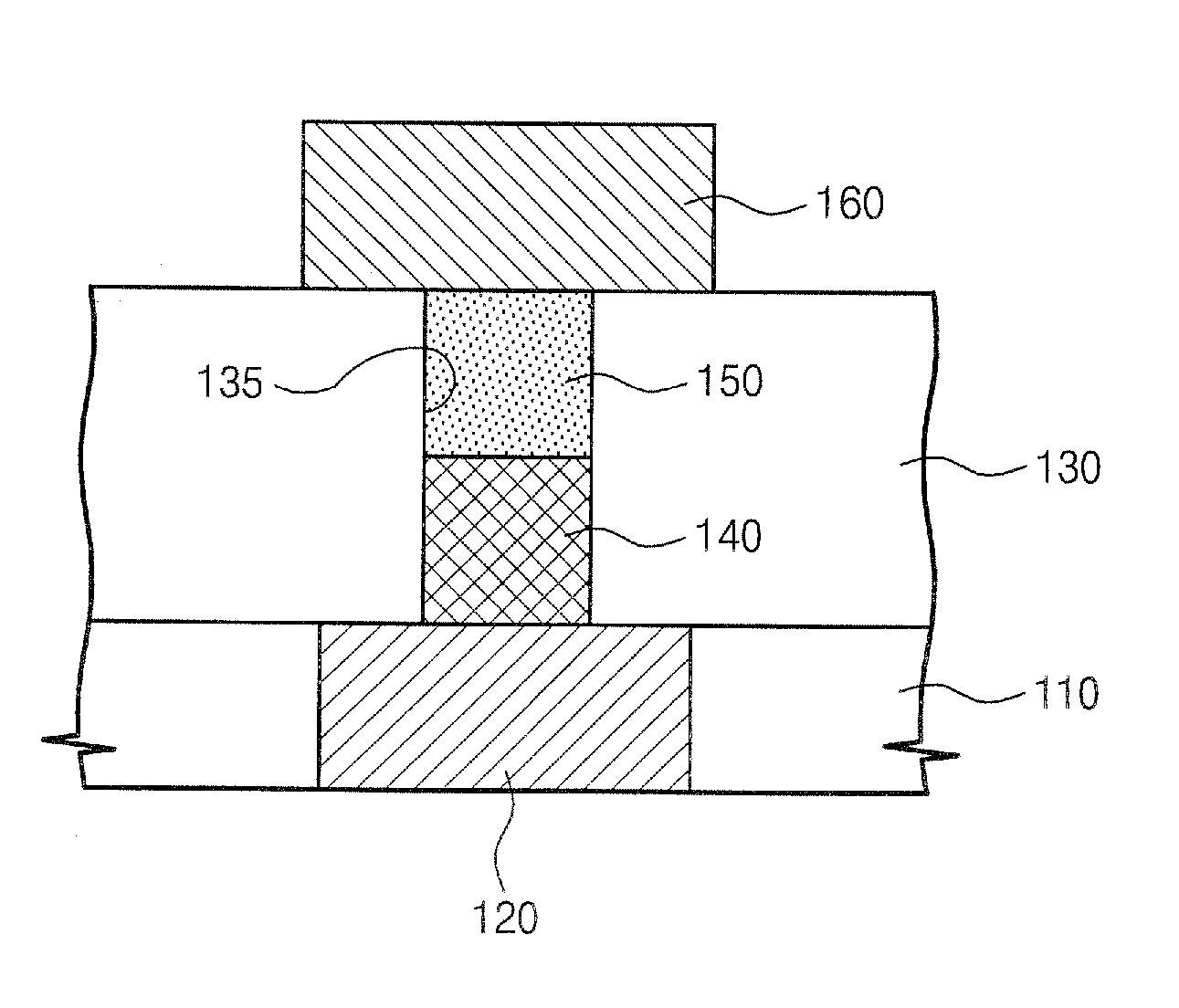
[0013] Another embodiment exemplarily described herein can be characterized as a method of forming a germanium compound that includes reacting tetra halide germanium GeX14 with a first chemical compound having a chemical formula R1MgX2 to generate a second chemical compound having a chemical formula GeR1xX1y and reacting the second chemical compound GeR1xX1y with a third chemical compound having a chemical formula LiR2 or a fourth chemical compound having a chemical formula R2MgX3 to generate a fifth chemical compound having a chemical formula GeR1xR2y. “R1” is an alkyl group, and “R2” is one of hydrogen, an amino group, an allyl group and a vinyl group. Each of “X1”, “X2” and “X3” may be a halogen element. “x” may be greater than zero and less than 4 and sum of “x” and “y” may be equal to 4. In one embodiment, the tetra halide germanium GeX14 may be tetra chloro germanium GeCl4. In another embodiment, “R1” may include iso-propyl. In another embodiment, the amino group may be NR3R4, and each of R3 and R4 may be an alkyl group. “R3” may be one of methyl, ethyl, iso-propyl and tert-butyl, and “R4” may be one of methyl, ethyl, iso-propyl and tert-butyl.
[0014] Yet another embodiment exemplarily described herein can be characterized as a method of forming a semiconductor device that includes supplying a germanium precursor, an antimony precursor and a tellurium precursor toward a substrate to form a phase change material layer. The germanium precursor may be a germanium compound having a chemical formula GeR1xR2y. “R1” may be an alkyl group and “R2” may be one of hydrogen, an amino group, an allyl group and a vinyl group. “x” may be greater than zero and less than 4, and sum of “x” and “y” equal to 4. In one embodiment, “R1” may comprise iso-propyl. In another embodiment, the amino group may comprise NR3R4, and each of “R3” and “R4” may be an alkyl group. “R3” may be one of methyl, ethyl, iso-propyl and tert-butyl, and “R4” may be one of methyl, ethyl, iso-propyl and tert-butyl. In another embodiment, the antimony precursor may be tri iso-propyl antimony (Sb(C3H7)3). In another embodiment, the tellurium precursor may be tert butyl tellurium (Te(C4H9)2). In another embodiment, the germanium precursor, the antimony precursor and the tellurium precursor may be supplied by periodically supplying a first source material containing the germanium precursor and the tellurium precursor and periodically supplying a second source material containing the antimony precursor and the tellurium precursor. The first and second source materials may be alternately supplied. In another embodiment, an insulating layer having an opening therein may be formed before forming the phase change material layer. In this case, the phase change material layer may be formed in the opening. The opening may have a width of about 100 nm or less. In addition, a conductive plug may be formed in the lower region of the opening before forming the phase change material layer. In still another embodiment, the phase change material layer may be formed by performing a chemical vapor deposition process or an atomic layer deposition process at a process temperature of about 250° C. to about 350° C. The process temperature may be equal to or lower than about 325° C.
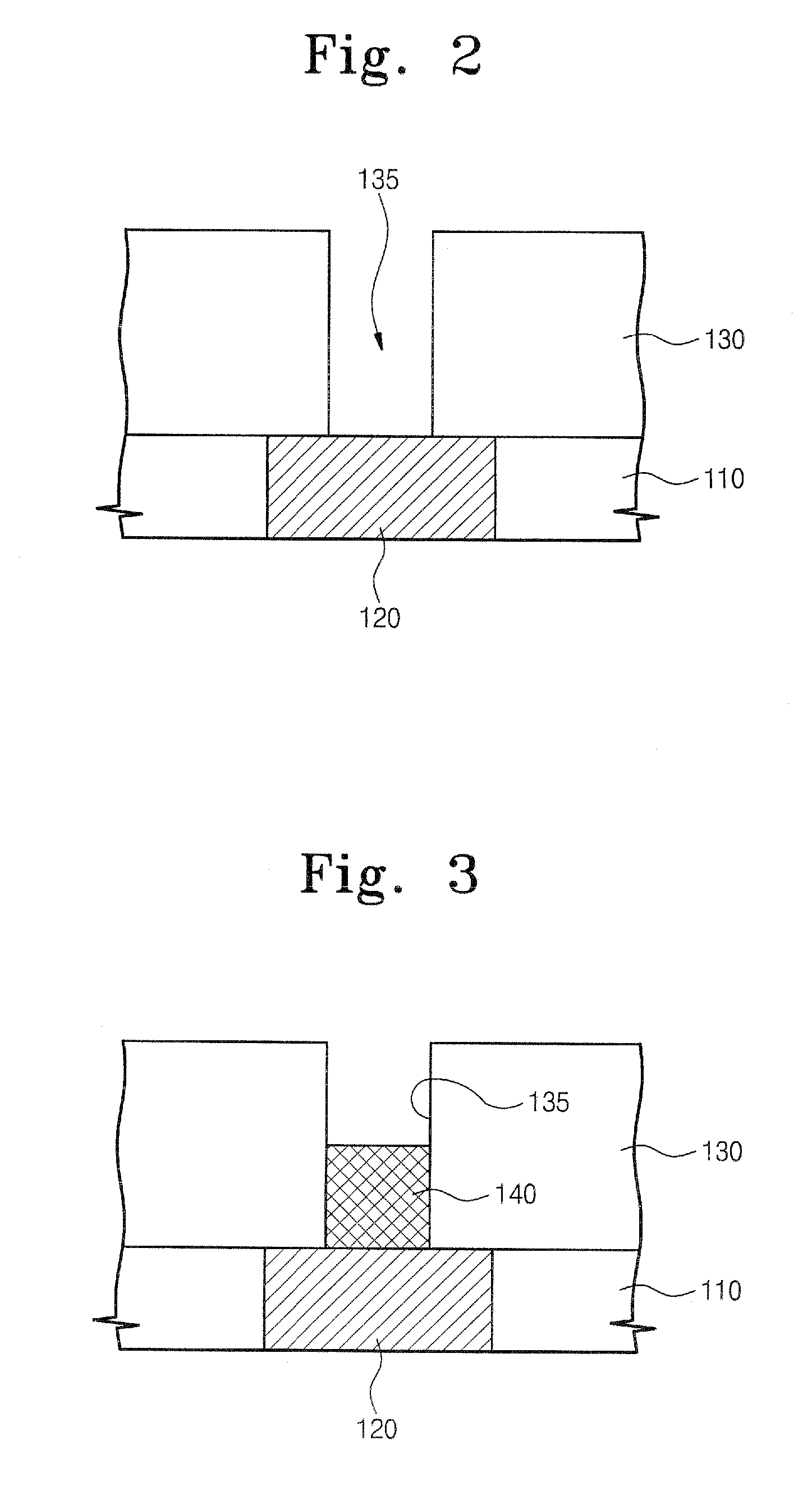
[0015] A further embodiment exemplarily described herein can be characterized as a semiconductor device that includes a substrate including a conductive region and an insulating layer on the substrate. The insulating layer may include an opening that exposes the conductive region. A phase change material pattern may be located in the opening. A top surface of the phase change material pattern may be substantially coplanar with or lower than a top surface of the insulating layer. In one embodiment, the phase change material pattern may have a width of about 100 nm or less. In other embodiments, a conductive plug may be provided between the phase change material pattern and the conductive region. In yet other embodiments, a conductive pattern may be disposed on the phase change material pattern.

Problems solved by technology

Data stored within volatile memory devices is lost when power is not supplied to the memory device.
However, nonvolatile memory devices retain stored data even in the absence of power.
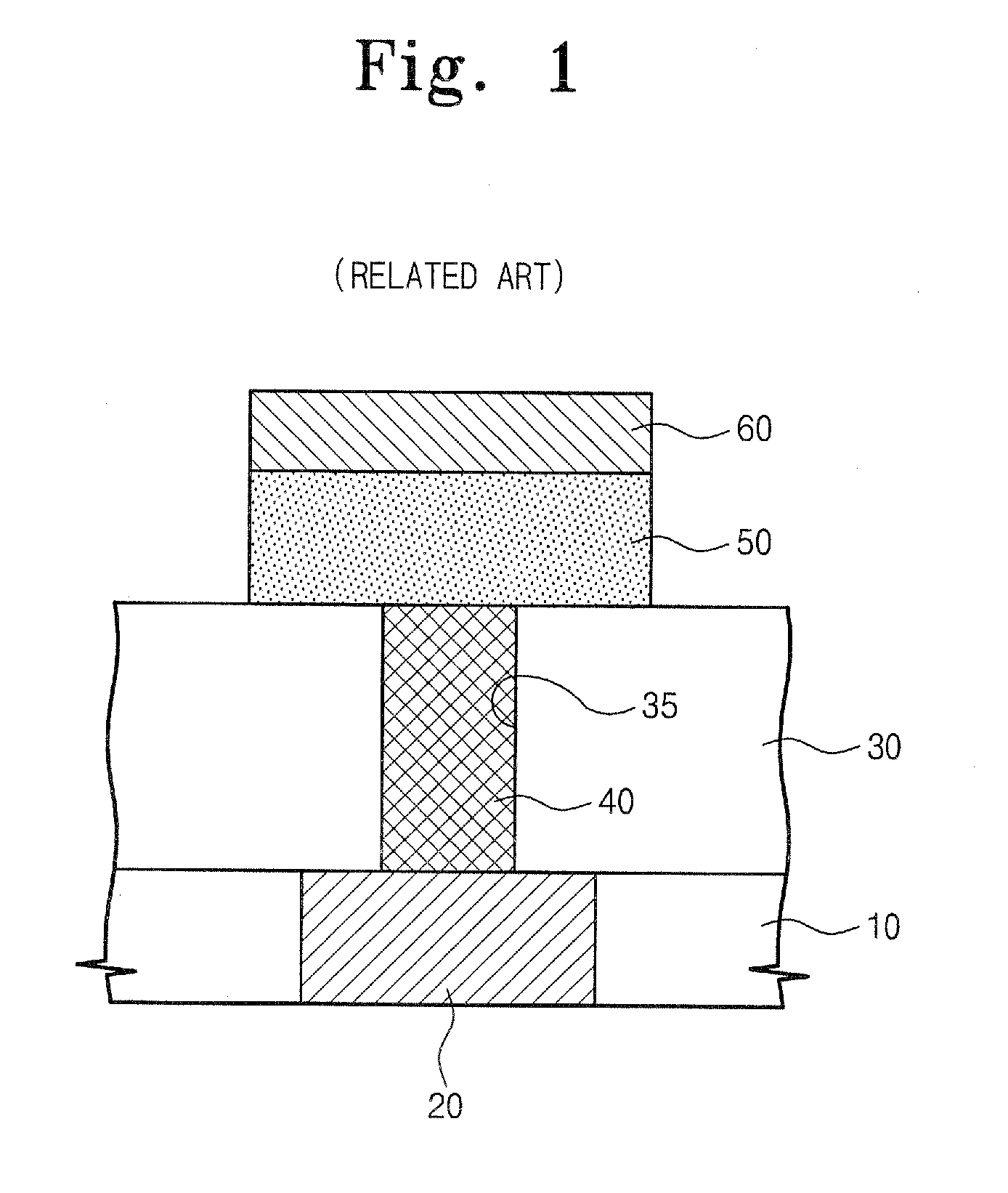
However, when the phase change material pattern 50 is formed using the photolithography process and the etching process as described above, there may be a limitation in reducing the size of the phase change material pattern 50.
Accordingly, it may be difficult to form small phase change material patterns having a width less than about 100 nm using the conventional photolithography and etching processes.
Therefore, it is difficult to reduce power consumption, which is required to change the crystalline structure of the phase change material pattern 50.
However, when the phase change material pattern is formed in the opening using conventional CVD techniques, the phase change material pattern may be non-uniformly formed within the opening.

Method used


Image

  • Germanium compound, semiconductor device fabricated using the same, and methods of forming the same
  • Germanium compound, semiconductor device fabricated using the same, and methods of forming the same
  • Germanium compound, semiconductor device fabricated using the same, and methods of forming the same

Examples


embodiment 1

[0043] In Embodiment 1, a germanium compound may be formed by first reacting about 3.5 moles of magnesium and about 3.1 moles of isopropyl bromine with each other in about 3 liters of ethyl ether for two hours and removing unreacted magnesium to provide an isopropyl bromomagnesium ((iso-C3H7)MgBr) solution. Tetra-chloro germanium (GeCl4) may then be added into the isopropyl bromomagnesium ((iso-C3H7)MgBr) solution and the tetra-chloro germanium (GeCl4) and the isopropyl bromomagnesium ((iso-C3H7)MgBr) may then be reacted with each other at a temperature of about 130° C. for about 12 hours. In one embodiment, the isopropyl bromomagnesium ((iso-C3H7)MgBr) solution may be refluxed with the tetra-chloro germanium (GeCl4) during the reaction. The reaction of the isopropyl bromomagnesium ((iso-C3H7)MgBr) and the tetra-chloro germanium (GeCl4) may be expressed by the following reaction formula 3.

GeCl4+(iso-C3H7)MgBr→Ge(iso-C3H7)Cl3+MgBrCl   (reaction formula 3)

[0044] The solution generat...

embodiment 2

[0047]FIG. 6 is a timing diagram to illustrate a method of forming a phase change material layer according to one embodiment.

[0048] Referring to FIG. 6, a Ge precursor, a Sb precursor and a Te precursor are provided on a substrate. The germanium compound (for example, Ge(iso-C3H7)(N(C2H5)(CH3))3) described above with respect to Embodiment 1 may be used as the Ge precursor, tri iso-propyl antimony (Sb(C3H7)3) may be used as the Sb precursor, and tert-butyl tellurium (Te(C4H9)2) may be used as the Te precursor.

[0049] In one embodiment, a first source material containing the Ge and Te precursors and a second source material containing the Sb and Te precursors may be alternately and repeatedly supplied to perform a chemical vapor deposition (CVD) process. Each of the first and second source materials may be supplied for about one second. A purge gas may be supplied during the CVD process. The purge gas may include, for example, argon (Ar) gas and hydrogen (H) gas. The CVD process may ...


PUM

PropertyMeasurementUnit
widthaaaaaaaaaa
temperatureaaaaaaaaaa

Abstract

A germanium (Ge) compound is provided. The Ge compound has a chemical formula GeR1xR2y. “R1” is an alkyl group, and “R2” is one of hydrogen, amino group, allyl group and vinyl group. “x” is greater than zero and less than 4, and the sum of “x” and “y” is equal to 4. Methods of forming the Ge compound, methods of fabricating a phase change memory device using the Ge compound, and phase change memory devices fabricated using the Ge compound are also provided.

Description

CROSS-REFERENCE TO RELATED APPLICATION [0001] This application claims the benefit of foreign priority to Korean Patent Application No. 10-2006-0065987, filed Jul. 13, 2006, the disclosure of which is hereby incorporated herein by reference in its entirety. BACKGROUND [0002] 1. Field of Invention [0003] Embodiments of the present invention relate generally to chemical compounds, semiconductor devices fabricated using such chemical compounds and methods of forming such semiconductor devices. More particularly, embodiments of the present invention relate to a germanium compound, a semiconductor device fabricated using the germanium compound and methods of fabricating such a semiconductor device. [0004] 2. Description of the Related Art [0005] Volatile memory devices and nonvolatile memory devices are types of semiconductor devices. Data stored within volatile memory devices is lost when power is not supplied to the memory device. However, nonvolatile memory devices retain stored data e...

Claims


Application Information

Patent Timeline
Patent Type & Authority Applications(United States)
IPC IPC(8): H01L47/00C07F7/30H01L21/06
CPCC07F7/30C23C16/305H01L45/06H01L45/1683H01L45/144H01L45/1616H01L45/1233H10N70/231H10N70/023H10N70/8828H10N70/826H10N70/066G11C13/0004
Inventor PARK, HYE-YOUNGKIM, MYONG-WOONKIM, JIN-DONGLEE, CHOONG-MANLEE, JIN-IL
Owner SAMSUNG ELECTRONICS CO LTD
Learn More