

Silicon Epitaxial Wafer And Manufacturing Method Thereof
a technology of silicon epitaxial wafers and manufacturing methods, which is applied in the direction of transportation and packaging, under a protective fluid, after-treatment details, etc., can solve the problems of inability to stably form oxygen precipitation nuclei at a density of 110sup>10 /sup>cmsup>3 /sup>or higher, and achieves a high possibility of rapid increase in deformation, excessive increase of the density of oxygen
- Summary
- Abstract
- Description
- Claims
- Application Information
AI Technical Summary
Benefits of technology
Problems solved by technology
Method used
Image

Examples
example 1
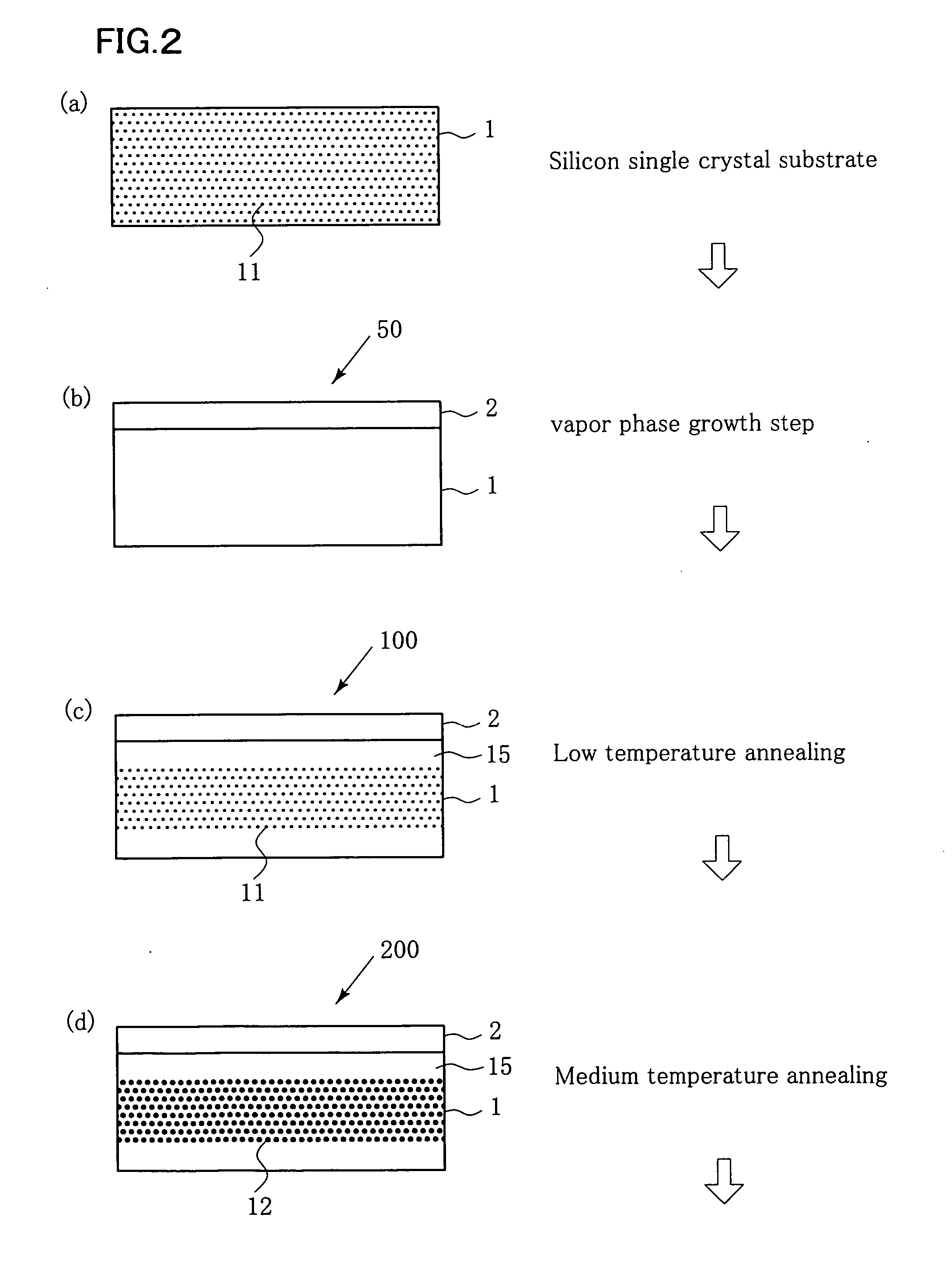
[0032] Descriptions will be given more specifically with examples below. Note that an initial oxygen concentration in a silicon single crystal substrate 1 described in the example is usually expressed as a conversion of a measured value by means of an inert gas fusion method, based on a correlation between a Fourier transform infrared spectroscopy and an inert gas fusion method, obtained using a substrate with an ordinary resistivity in the range of 1 to 20 Ω·cm. A density of oxygen precipitation nuclei 11 is measured in the following way: the medium temperature annealing is further applied to the silicon epitaxial wafer 100 in which oxygen precipitation nuclei 11 have been produced to thereby mature the nuclei 11 into oxygen precipitates 12 and thereafter, the silicon epitaxial wafer is applied to selective etching using an etching solution including hydrofluoric acid (with a concentration in the range of 49 to 50 wt %): nitric acid (with a concentration in the range of 60 to 62 wt...
example 2
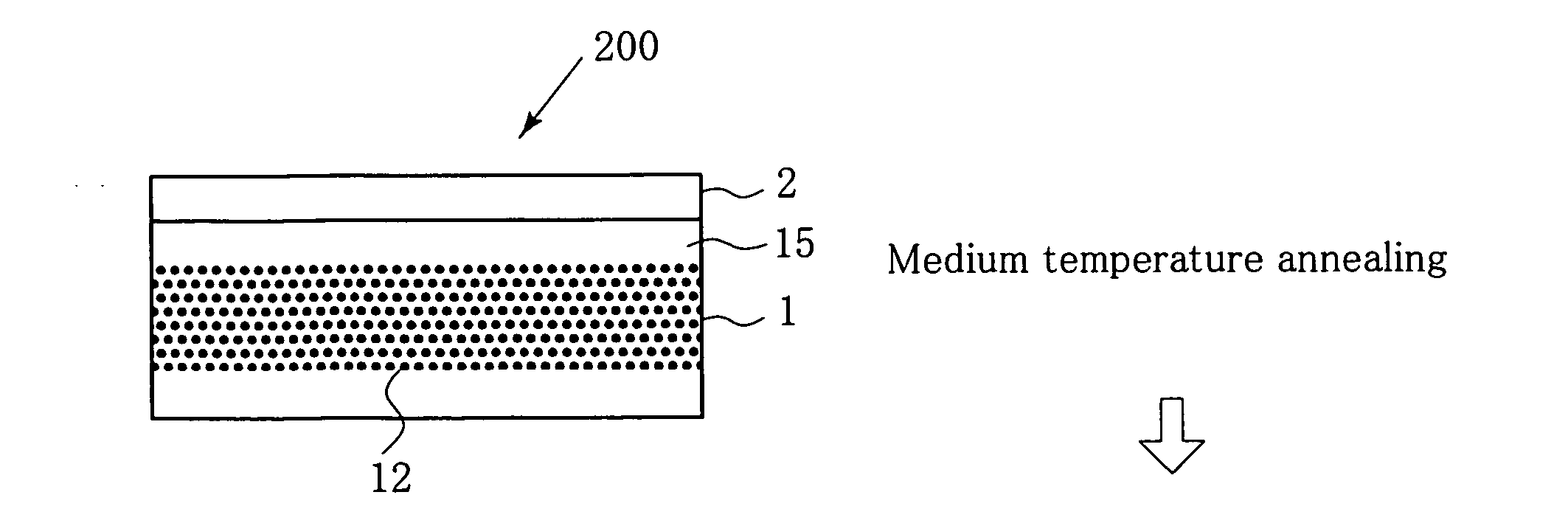
[0036] In FIG. 3, there is shown a relationship between a substrate resistivity and a width of a no-oxygen-precipitation-nucleus-forming-region in a process where low temperature annealing at 650° C. for 1 hr and medium temperature annealing under conditions of 800° C. for 4 hr and 1000° C. for 16 hr in this order were applied to silicon epitaxial wafers 50 manufactured, as described above, using p+ CZ substrates 1 with various resistivities. It can be seen that a width of a no-oxygen-precipitation-nucleus-forming-region 15 can be decreased to 10 μm or less in a case of a substrate resistivity of 0.012 Ω·cm or less.
[0037] In FIG. 4, there is shown a relationship between a substrate resistivity and an initial oxygen concentration of the substrate, and it shows that with a lower substrate resistivity, the initial oxygen concentration increases. This means that with a lower substrate resistivity, more oxygen precipitates can be produced and also that a width of a no-oxygen-precipitati...
PUM
 Abstract
Description
Claims
Application Information