Method for fabricating micro and NANO structures

a nano-structure and nano-technology, applied in the field of optical device fabrication, to achieve the effect of reducing particle size and particle siz

Inactive Publication Date: 2008-02-28
AGENCY FOR SCI TECH & RES
View PDF6 Cites 39 Cited by
  • Summary
  • Abstract
  • Description
  • Claims
  • Application Information

AI Technical Summary

Benefits of technology

[0013] In a third aspect, the invention provides a method of forming an array of selectively shaped optical elements on a substrate, the method comprising the steps of: providing the substrate, said substrate having an optical layer placed thereon; placing a layer of particles on the optical layer; performing an etching cycle, said cycle comprising the steps of: etching the layer of particles, using a first etching proce

Problems solved by technology

Second, surface structures are fabricated by dry et

Method used


Image

  • Method for fabricating micro and NANO structures
  • Method for fabricating micro and NANO structures
  • Method for fabricating micro and NANO structures

Examples


embodiment 1

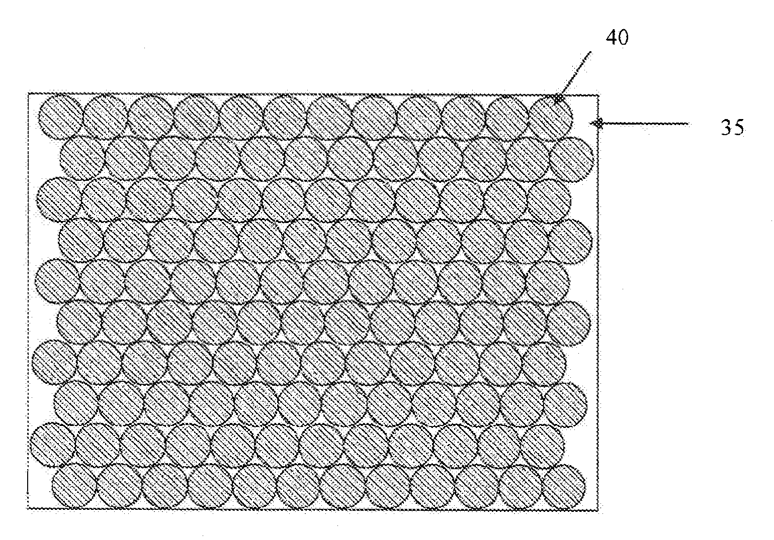
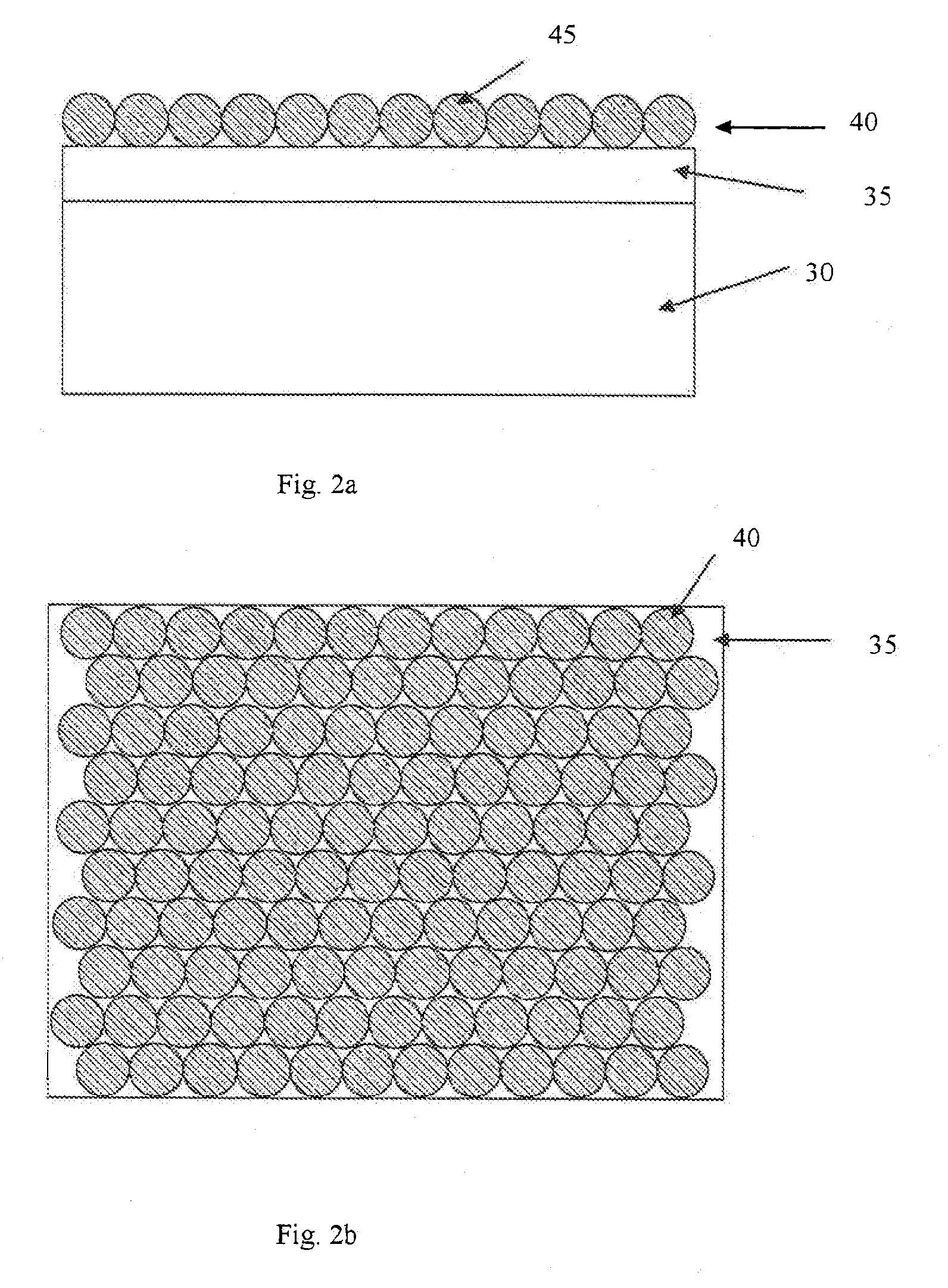
[0035] In a first embodiment, as shown in FIG. 2, the LED wafer 30 uses GaAs as a substrate, having a p type top layer 35, beside an active layer of multi quantum wells, a pair of n and p type cladding layers and a Bragg reflector grown by MOCVD. The material of the p type top layer is GaP with thickness being around 5 micrometer. The wavelength of light emitted from the LED wafer is around 635 nanometer (nm). Following the procedure indicated in FIG. 1, the surface of the wafer is treated 5 by ozone at 130° C. for 10 min, resulting in the surface to be hydrophilic. A monolayer 40 of polystyrene (PS) spheres 45 with mean diameter of 600 nm is self-assembled 10 on the top layer 35 from colloidal suspension of PS spheres purchased from a company, which is diluted to be around 20% w / w before deposition. It should be noted, that the invention may equally apply for particles in the range 100 nm to 10 μm.

[0036] A simple method to deposit 10 the PS spheres is used in these experiments. Se...

embodiment 2

[0040] In a second embodiment, in order to obtain different section profiles of the etched structures, multi etching cycles 25 of RIE and ICP are used alternatively (multi-etching-cycle). FIGS. 5(a), (b) and (c) show some possible structures 70, 80, 90 that can be obtained by the invention using multi-etching-cycle process just simply changing etching durations at different etching steps.

[0041] For the following experiments, the etching conditions are kept the same as described in Embodiment 1 for all etchings, but the etching duration. The LED wafers and layering the monolayered PS spheres 40 on the LED wafer 30 are also similar to that mentioned in the Embodiment 1. Only the etching durations of RIE and ICP are varied to control the cross-section profiles of the etched structures on the top layer 35 of the LED wafer 30.

[0042] Examples of Embodiment 2 are shown in FIG. 7(a), top-view and 7(b) tilted view of SEM images showing the surface structures fabricated by multi-etching-cyc...

embodiment 3

[0047] In a third embodiment, a GaN-base LED wafer is used and the top layer is p type GaN material (˜300 nm thick). The wavelength of light emitted from the LED wafer is around 570 nm. A thin hydrophilic SiO2 film with thickness of ˜30 nm is deposited by PECVD on the surface of the wafer in order to arrange the PS spheres. The same sized PS spheres and it's self-assembling into monolayer process as mentioned in Embodiment 1 are used for the wafer.

[0048] After arranging the monolayered PS spheres on the wafer, it is then loaded into an ICP chamber to create the surface nanostructures. Oxygen RIE at the conditions: O2 flow, 20 sccm, RIE power, 200 W, chamber pressure, 8 mTorr is used for etching the PS spheres to reduce their diameters, while ICP with mixed BCl3 and Cl2 at the conditions: BCl3: 20 sccm, Cl2, 10 sccm, RIE power, 200 W, ICP power, 500 W, chamber-press, 8 mTorr is used for p-GaN material as well as the PS sphere etching. In this case, the average etching rates for p-Ga...


PUM

PropertyMeasurementUnit
Dielectric polarization enthalpyaaaaaaaaaa
Sizeaaaaaaaaaa
Ratioaaaaaaaaaa

Abstract

A method of forming an array of selectively shaped optical elements on a substrate, the method including the steps of providing the substrate, the substrate having an optical layer placed thereon; placing a layer of particles on the optical layer; performing an etching cycle. The cycle includes the steps of: etching the layer of particles, using a first etching process so as to reduce the size of the particles within the layer, then; simultaneously etching the optical layer and the layer of particles, using a second etching process, the further reducing particles forming a mask over areas of the optical layer to create discrete optical elements from the optical layer.

Description

FIELD OF THE INVENTION [0001] The invention relates to the fabrication of optical devices, including but not limited to LED's, light detectors, photovoltaic cells etc. In particular, the invention relates to the fabrication of common sub-elements within such devices. BACKGROUND [0002] Light emitting diodes (LEDs) are typically constructed by growing a p-n diode on a substrate. The diode is constructed by growing a layer of n-doped material on the substrate, growing a light generation region on the n-doped layer, and then growing the layer of p-doped material on top of the n-doped material. An electrode is then deposited on the top surface of the p-doped layer, and a contact is made to the n-doped layer. Light may be extracted either through the substrate or through the top surface of the p-doped material or through the top electrode. If the light is to be removed through the top electrode, the electrode is constructed from a transparent material such as indium tin oxide or thin gold...

Claims


Application Information

Patent Timeline
IPC IPC(8): B29D11/00H01L33/06
CPCB29D11/00365B82Y20/00B82Y30/00G02B3/0012G02B3/0056Y10S977/888Y10T428/24165Y10T428/24893Y10T428/24909
Inventor WANG, BENZHONGCHUA, SOO JIN
Owner AGENCY FOR SCI TECH & RES
Why Eureka
Try Eureka