Noise-suppressing wiring-member and printed wiring board

a technology of wiring-member and wiring board, which is applied in the direction of cross-talk/noise/interference reduction, electrical apparatus contruction details, and association of printed circuit non-printed electric components, etc., which can solve the problems of simultaneous switching noise in the power supply layer and the ground layer, and the inability to acquire such a material

Active Publication Date: 2008-02-28
SHIN-ETSU POLYMER CO LTD
View PDF7 Cites 70 Cited by
  • Summary
  • Abstract
  • Description
  • Claims
  • Application Information

AI Technical Summary

Benefits of technology

[0160] A two-layered board composed of a ground layer and a power supply layer was prepared. At both ends of one of the power supply layer divided in two, SMA connectors linking to the power supply layer and the ground layer are mounted. S21 (transmission attenuation amount, unit: dB) was measured in accordance with a scattering parameter (S parameter) method using a network analyzer (manufactured by Anritsu Company under the trade name of 37247D) connected to the SMA connectors, and the resonance state of the S21 pa

Problems solved by technology

However, such a spread of these devices is becoming a controversial issue in that a radiation noise radiated from these devices and a conduction noise conducting through these devices cause malfunction of the devices, other electronic equipment, or parts thereof, and cause influences on the human body.
For example, when plural transistors in a semiconductor element mounted in a multilayer printed wiring board are simultaneously driven, unwanted high-frequency current flows in a power supply layer or a ground layer, as a result of which a potential variation occurs.
The potential variation causes simultaneous switching noise in the power supply layer and the ground layer.
Also, since the power supply layer and the ground layer have a parallel flat plate structure in which peripheral end parts thereof are opened, the potential variation causes resonance between the power supply layer and the ground layer, as a result of which radiation noise is radiated from the peripheral end parts.
However, it is practically impossible to acquire such a material, and thereby the printed wiring board (1) cannot exhibit sufficient noise suppressing effects.
However, a step of forming an anisotropically conductive film with a surface roughness of copper foil equal to or greater than the surface depth is complicated The printed wiring board (2) also cannot e

Method used


Image

  • Noise-suppressing wiring-member and printed wiring board
  • Noise-suppressing wiring-member and printed wiring board
  • Noise-suppressing wiring-member and printed wiring board

Examples


examples

[0157] In the following, the present invention will be explained in more detail with reference to Examples and Comparative Examples. However, it should be apparent that the present invention is not limited to these examples.

examples 1 to 3

(Thickness of Noise Suppressing Layer)

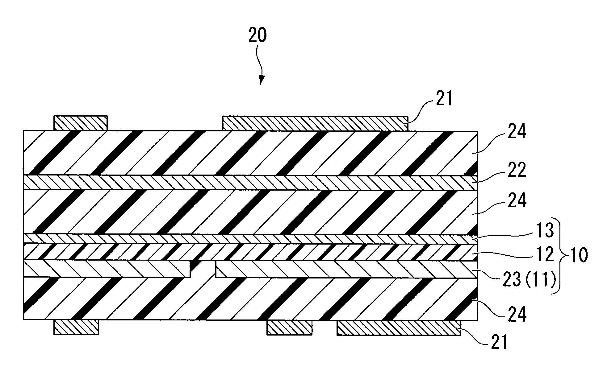
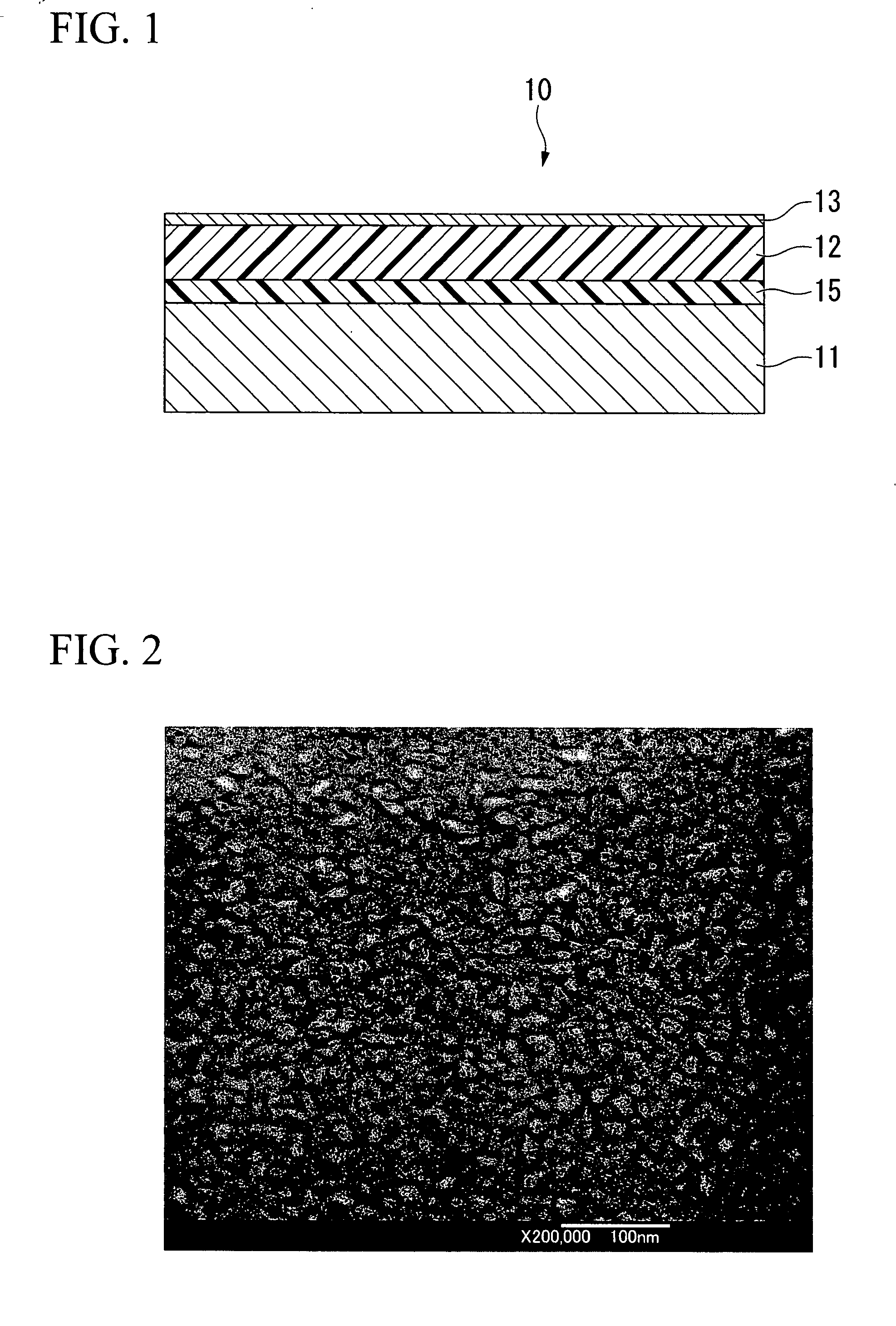
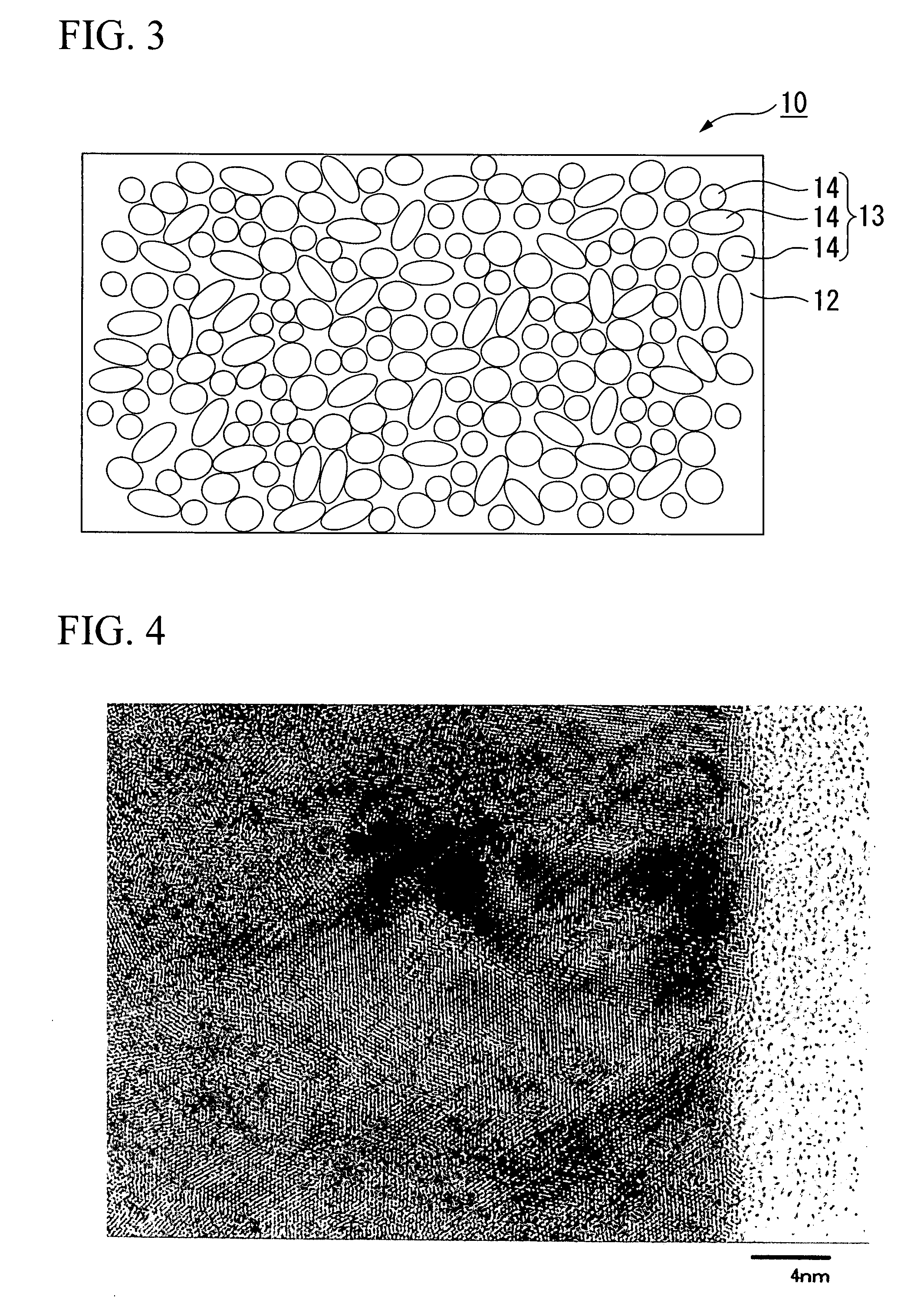
[0158] The thickness of a noise suppressing layer was measured at five points by observing a cross section of the noise suppressing layer using a transmission electron microscope manufactured by Hitachi, Ltd., under the trade name of H9000NAR and the measured values were averaged.

(Adhesive Strength)

[0159] The strength required for peeling a copper foil layer of a wiring member from an insulating resin layer was measured at a peeling rate of 50 mm / minutes and a peeling angle of 90° using a Tensilon tensile tester in accordance with JIS C5012.

(Noise Suppressing Effects)

[0160] A two-layered board composed of a ground layer and a power supply layer was prepared. At both ends of one of the power supply layer divided in two, SMA connectors linking to the power supply layer and the ground layer are mounted. S21 (transmission attenuation amount, unit: dB) was measured in accordance with a scattering parameter (S parameter) method using a network...

example 1

[0162] An electrolytic copper foil layer with a thickness of 35 μm had a smooth surface and a roughened surface. The surface roughness Rz of the smooth surface was 2 μm. In contrast, the surface roughness Rz of the roughened surface was 5.3 μm. On the smooth surface, a solution containing 1% by mass of 3-glycidoxypropyltrimethoxysilane was applied and dried to form an adhesion promoting layer.

[0163] 30 parts by mass of bisphenol A type epoxy resin (manufactured by Japan Epoxy Resins Co., Ltd., under the trade name of 828), 30 parts by mass of bromine bisphenol A type resin (manufactured by Tohto Kasei Co., Ltd., under the trade name of YDB-500), and 35 parts by mass of cresol novolac resin (manufactured by Tohto Kasei Co., Ltd., under the trade name of YDCN-704) were dissolved in methyl ethyl ketone. Then, 0.2 parts by mass of imidazole-based hardening accelerator (manufactured by Shikoku Chemicals Corporation, under the trademark of CUREZOL 2E4MZ) were added to the solution to pre...


PUM


Abstract

The present invention relates to a wiring member including: a copper foil layer having a smooth surface with a surface roughness Rz of 2 μm or less; a noise suppressing layer containing a metallic material or a conductive ceramic and having a thickness of 5 to 200 nm; and an insulating resin layer provided between the smooth surface of the copper foil layer and the noise suppressing layer, and also relates to a printed wiring board equipped with the wiring member. Moreover, the present invention relates to a noise suppressing structure including: a first conductive layer; a second conductive layer; a noise suppressing layer provided between the first conductive layer and the second conductive layer, the noise suppressing layer being to be electromagnetically-coupled with the first conductive layer, the noise suppressing layer comprising a metallic material or a conductive ceramic, and the noise suppressing layer having a thickness of 5 to 300 nm; a first insulating layer provided between the first conductive layer and the noise suppressing layer; and a second insulating layer provided between the second conductive layer and the noise suppressing layer; wherein the noise suppressing structure has: a region (I) in which the noise suppressing layer and the first conductive layer face each other; and a region (II) in which the noise suppressing layer and the first conductive layer do not face each other but the noise suppressing layer and the second conductive layer face each other, the regions (I) and (II) neighboring each other.

Description

BACKGROUND OF THE INVENTION [0001] 1. Field of the Invention [0002] The present invention relates to a noise-suppressing wiring-member for composing a printed wiring board and the printed wiring board. Also, the present invention relates to a noise suppressing structure and a multilayer printed wiring board. [0003] The present invention claims priority on Japanese Patent Application No. 2006-181179, filed on Jun. 30, 2006, and Japanese Patent Application No. 2006-199286, filed on Jul. 21, 2006, the content of which is incorporated herein by reference. [0004] 2. Description of the Related Art [0005] In recent years, a central processing unit (CPU) with a high clock frequency in a sub-microwave band (0.3 to 10 GHz), such as in a personal computer, personal digital electronics, local area wireless networks, Bluetooth, optical modules, mobile phones, game equipment, personal digital assistants, intelligent transport information systems, and the like, electronic equipment which utilizes ...

Claims


Application Information

Patent Timeline
IPC IPC(8): H05K9/00
CPCH05K1/0234H05K1/0298H05K1/167H05K2201/09309H05K2201/0317H05K2201/0326H05K2201/093H05K2201/0191H05K1/03
Inventor KAWAGUCHI, TOSHIYUKITAHARA, KAZUTOKISAGA, TSUTOMUNEGISHI, MITSUAKI
Owner SHIN-ETSU POLYMER CO LTD
Why Eureka
Try Eureka