Thin-film transistor and fabrication method thereof

a technology of thin film transistor and fabrication method, which is applied in the direction of thermoelectric device junction materials, semiconductor devices, electrical apparatus, etc., can solve the problems of inability to extend the length of the gate (i.e. tft channel resolution) to several micrometers and less, and achieve the effect of widening the application range and simplifying the process

Inactive Publication Date: 2008-03-06
IND TECH RES INST
View PDF5 Cites 20 Cited by
  • Summary
  • Abstract
  • Description
  • Claims
  • Application Information

AI Technical Summary

Benefits of technology

[0011]The invention utilizes the ridges of a ring profile to form a thin-film transistor (TFT) and the ring profile is formed by inkjet printing in combination with a coffee ring effect to achieve a simpler process and to widen an application range thereof.

Problems solved by technology

In general, the diameter of the drop on the substrate is from several tens to several hundreds of micrometers, and is thus too large for high resolution electronic devices.
These technologies, however, are unable to extend the length of a gate (i.e. TFT channel resolution) to several micrometers and less.
A micro-contact printing and a nanoimprinting are able to form a micro-line, however, in fabrication on a large sized substrate, these technologies have difficulties in repeated alignment and mass production.
Because there are no isolated lines formed by the described technology, it cannot be used for fabricating an electronic device.
The disadvantage of this fabrication method is that the film forming technology thereof is a higher cost vacuum deposition.
However, the coffee ring formed by inkjet printing has two ridges, if only one ridge is used, the gap between the device will be widened such that high density and high resolution fabrication is hindered.
The disadvantages of this method include an additional cost for a lift-off process.
At the same time, lift-off processes damage the surfaces of the source / drain electrodes.

Method used


Image

  • Thin-film transistor and fabrication method thereof
  • Thin-film transistor and fabrication method thereof
  • Thin-film transistor and fabrication method thereof

Examples


first embodiment

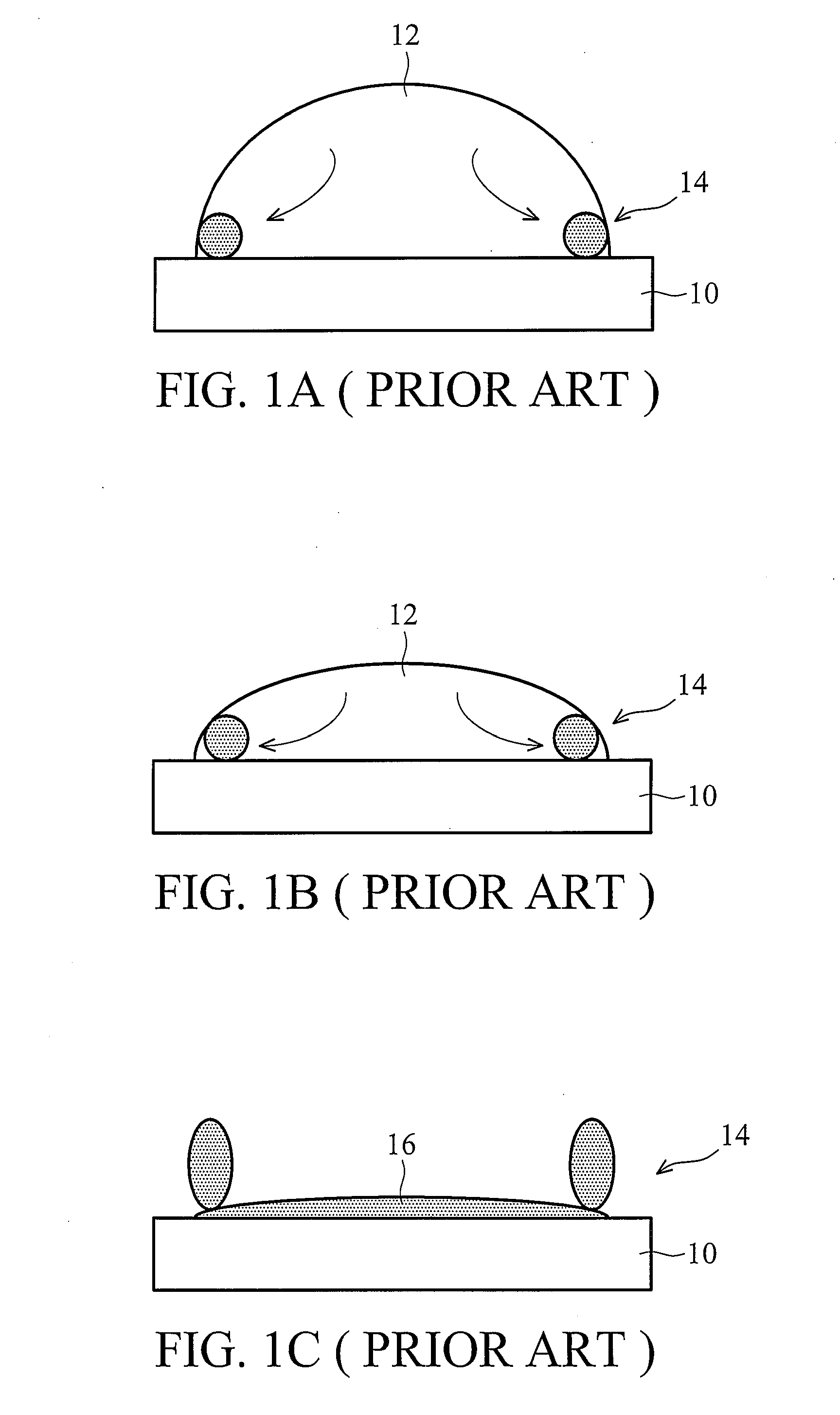
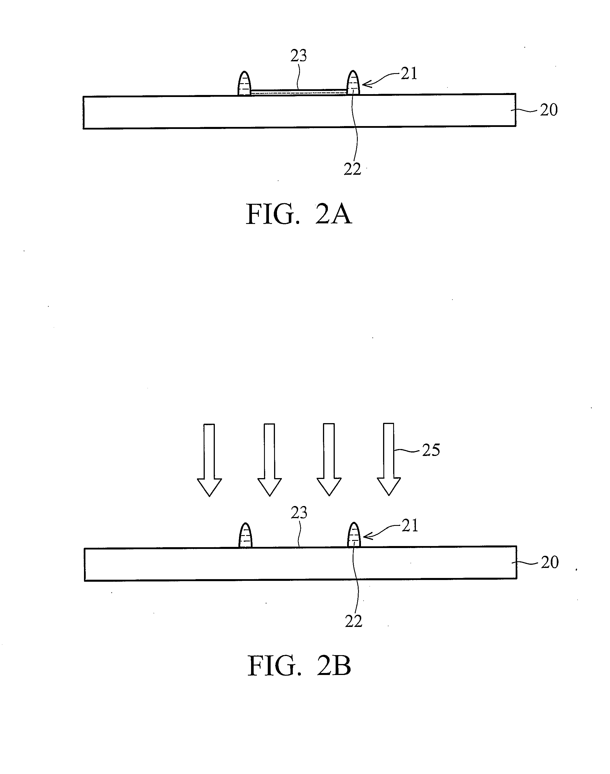
[0035]FIGS. 2A-2F show cross sections of fabrication steps of a first embodiment of the invention. Referring to FIG. 2A, a substrate 20, such as glass, silicon, plastic substrate or other flexible substrate, is first provided. The selected substrate is then cleaned and treated by a surface treatment step such as plasma treatment. A polymer solution is inkjet printed by a sprinkle-nozzle on the substrate 20 into a dot or a line shape, and then dried into a coffee ring film 21. The polymer may be, but is not limited to, poly(3-alkylthiophene) (P3AT), poly(9,9-dioctylfluorene-co-bithiophene) (F8T2), polymethyl methacrylate (PMMA), poly(4-vinylphenol) (PVP), polyvinyl alcohol (PVA), polyacrylonitrile (PAN), polyimide (PI), or polyoxymethylene (POM). The polymer is dissolved in a solvent into a solution for inkjet printing. The solvent includes a watery liquid or an oily liquid.

[0036]Referring to FIG. 2B, a central part 23 of the coffee ring film 21 is removed by an etching method, and t...

second embodiment

[0044]In the second embodiment of the invention, the different semiconductor materials are inkjet printed on the two ridges, one is N type semiconductor, and the other is P type semiconductor, thus completing a CMOS TFT structure.

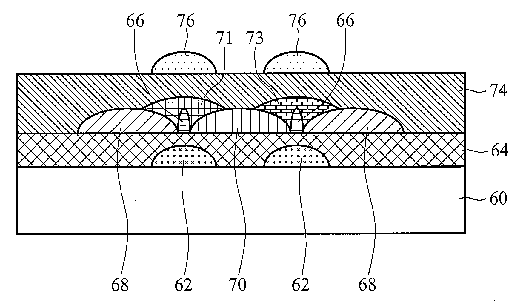
[0045]As shown in FIG. 5, a substrate 20 is first provided, and then two ridges 22 of the coffee ring are formed on the substrate 20 as a separating layer. A source layer 24 and a drain layer 26 are disposed on opposite sides of the ridge 22. A P type semiconductor layer 27 is disposed on one ridge 22 and portions of the source / drain layer. An N type semiconductor layer 29 is disposed on the other ridge 22 and portions of the source / drain layer. A gate dielectric layer 30 is disposed on the P type semiconductor layer 27, the N type semiconductor layer 29, the source layer 24 and the drain layer 26. A gate layer 32 is disposed on the gate dielectric layer 30, corresponding to the ridges 22. In the second embodiment, with the exception of the P type semicondu...

third embodiment

[0046]According to the structure of the first embodiment, wherein the substrate can be replaced by a substrate having a conductive layer and an inorganic gate dielectric layer, and the upper gate layer and the upper gate dielectric layer can be removed to form a bottom gate device.

[0047]The third embodiment of the invention is as shown in FIG. 6. A substrate 40 is first provided. A bottom gate layer 42 is disposed on the substrate 40, and the patterning process thereof is not required. The material of the bottom gate layer 42 may be a heavily doped N type or P type semiconductor such as a heavily doped Si, Ge, or GaAs; an organic conductive film such as PEDOT; or a metal or an inorganic conductive film such as ITO, IZO, Ag, Au, Al, or Cr. A bottom gate dielectric layer 44 is disposed above the bottom gate layer 42, and underlying a separating layer 46 and a source / drain layer 48 / 50. The material of the bottom gate dielectric layer 44 may be an inorganic insulating material, an organ...


PUM


Abstract

A thin-film transistor and fabrication method thereof are provided. A controlled micro-line is formed by inkjet printing in combination with the coffee ring effect. At least two organic thin-film transistors are formed on two ring ridges of the coffee rings. For example, N-type and P-type soluble semiconductor materials may be formed on two adjacent ring ridges to form a complementary metal-oxide semiconductor (CMOS) device. Thus, the invention can simplify the process for fabricating thin-film transistors and increase their applications.

Description

FIELD OF THE INVENTION[0001]The invention relates to a thin-film transistor, and more particularly to a thin-film transistor formed by inkjet printing in combination with the coffee ring effect.[0002]2. Description of the Related Art[0003]Organic polymer material is stable and soluble, thus, a solution of polymer material be utilized in fabricating products by dispensing. The process of dispensing method is simple and the cost thereof is reduced largely. The dispensing method is simple and the cost is relatively low.[0004]Micrometer scale drops can be formed on a substrate by inkjet printing of pico volume droplets, thus, a micrometer sized electronic device can be fabricated. In general, the diameter of the drop on the substrate is from several tens to several hundreds of micrometers, and is thus too large for high resolution electronic devices.[0005]A mechanism for forming coffee rings is shown in FIG. 1A to FIG. 1C. The mechanism can be referenced in Nature, Vol. 389, 1997, Rober...

Claims


Application Information

Patent Timeline
Patent Type & Authority Applications(United States)
IPC IPC(8): H01L51/00H01L51/40
CPCH01L27/281H01L27/283H01L51/102H01L51/0545H01L51/0004H10K19/201H10K19/10H10K71/13H10K10/466H10K10/82
Inventor TSAI, HSUAN-MINGLEE, YUH-ZHENGCHENG, CHAO-KAILU, JHIH-PINGLIN, KUO-TONG
Owner IND TECH RES INST
Why Eureka
Try Eureka