Semiconductor device and method of manufacturing semiconductor device

a semiconductor and semiconductor technology, applied in the direction of semiconductor devices, electrical devices, transistors, etc., can solve the problems of achieving both the suppression of short channel effect and the improvement of mobility, and achieve the reduction of threshold voltage, the increase of the permissible range of gate length variations, and the reduction of sheet carrier density

Active Publication Date: 2008-03-06
SONY CORP
View PDF4 Cites 23 Cited by
  • Summary
  • Abstract
  • Description
  • Claims
  • Application Information

AI Technical Summary

Benefits of technology

[0027]In the manufacturing method according to the above-described embodiment, the extension region is formed on the semiconductor substrate on both sides of the dummy gate. Thus a first semiconductor face (a face of the semiconductor substrate) and a second semiconductor face (a face of the extension region on a drain side) connected to each other at an angle are formed by the semiconductor substrate and the extension region on the drain side. The overlap region of the source impurity region is formed in the semiconductor substrate in such a manner as to overlap the gate electrode within the first semiconductor face with the gate insulating film interposed between the overlap region of the source impurity region and the gate electrode. Therefore a decrease in sheet carrier density in a gate corner part on a source side is avoided. In addition, the drain impurity region is formed in the semiconductor substrate under the second semiconductor face including the extension region on the drain side. Therefore a surface potential in the vicinity of a bend part of a channel (the first semiconductor face and the second semiconductor face) can be made higher than that of other parts. Thereby a drain electric field is shielded in the vicinity of the bend part. Thus a decrease in threshold voltage due to a short channel effect is suppressed, and a permissible range of variations in gate length is increased. Further, the overlap region of the source impurity region is formed, and thereby the junction interface between the drain impurity region and the semiconductor region is formed in a state of being closer to the boundary between the first semiconductor face and the second semiconductor face than the junction interface between the source impurity region and the semiconductor region. Therefore a decrease in local sheet carrier density in the vicinity of the bend part on the drain side is avoided, and a voltage drop in the vicinity of the bend part is suppressed. A semiconductor device having such characteristics is manufactured.
[0028]According to an embodiment of the present invention, there is provided a semiconductor device formed by a static random-access memory using an insulated gate field effect transistor as a selection transistor of a cell, the insulated gate field effect transistor including a semiconductor region having a first semiconductor face and a second semiconductor face connected to the first semiconductor face and having an inclination with respect to the first semiconductor face, a gate insulating film formed on the first semiconductor face and on the second semiconductor face, a gate electrode formed on the gate insulating film including a part on a boundary between the first semiconductor face and the second semiconductor face, a source impurity region formed in the semiconductor region so as to overlap the gate electrode within the first semiconductor face with the gate insulating film interposed between the source impurity region and the gate electrode, and a drain impurity region formed in the semiconductor region directly under the second semiconductor face at least, wherein a junction interface between the drain impurity region and the semiconductor region is formed in a state of being closer to the boundary between the first semiconductor face and the second semiconductor face than a junction interface between the source impurity region and the semiconductor region, a side of the source impurity region is connected to a bit line, and a side of the drain impurity region is connected to a gate electrode of a cell transistor.
[0029]In the semiconductor device according to the above-described embodiment, the insulated gate field effect transistor according to an embodiment of the present invention is used as the selection transistor of the cell. Therefore a high current driving power and a low leakage current are obtained in an inverter inside the cell. In addition, a threshold voltage on a drain side of the selection transistor is higher than on a source side due to action in the vicinity of a bend part between the first semiconductor face and the second semiconductor face. Therefore, when the inverter charges the bit line as a large capacitive load, a bit line side becomes a low threshold value side, and a high current driving power is obtained. When the gate of the inverter is conversely charged from the bit line, the drain side of the selection transistor is at a low potential, a high threshold value is obtained, and the current driving power is lowered. However, because a load to be charged is only a pair of gates, a disadvantage in terms of speed is insignificant.
[0030]According to an embodiment of the present invention, a decrease in sheet carrier density in the gate corner part on the source side is avoided. It is thus possible to prevent a rise in potential at the source end of the channel, and reduce a decrease in on current. In addition, the drain electric field is shielded in the vicinity of the bend part. Thus advantages are obtained in that a decrease in threshold voltage due to the short channel effect is suppressed and the permissible range of variations in gate length is increased. Further, a decrease in local sheet carrier density in the vicinity of the bend part on the drain side is avoided, and thus a voltage drop in the vicinity of the bend part can be suppressed. Thereby most of drain voltage is applied between the source and the vicinity of the bend part between the first semiconductor face and the second semiconductor face. Therefore a high current driving power is obtained.
[0031]According to an embodiment of the present invention, a decrease in sheet carrier density in the gate corner part on the source side is avoided. It is thus possible to prevent a rise in potential at the source end of the channel, and reduce a decrease in on current. In addition, the drain electric field is shielded in the vicinity of the bend part. Thus advantages are obtained in that a decrease in threshold voltage due to the short channel effect is suppressed and the permissible range of variations in gate length is increased. Further, a decrease in local sheet carrier density in the vicinity of the bend part on the drain side is avoided, and thus a voltage drop in the vicinity of the bend part can be suppressed. Thereby most of drain voltage is applied between the source and the vicinity of the bend part between the first semiconductor face and the second semiconductor face. Therefore a high current driving power is obtained. A semiconductor device having such characteristics can be manufactured.
[0032]According to an embodiment of the present invention, a high current driving power and a low leakage current are obtained in the inverter inside the cell. Therefore, a time for charging the bit line and a gate in a following stage can be shortened, and also static current consumption can be reduced. In addition, the selection transistor can obtain a high current driving power, and thus charge the bit line quickly. Thus the performance of the static random-access memory is enhanced.

Problems solved by technology

A problem to be solved is a difficulty in achieving both the suppression of the short channel effect and the improvement of mobility.

Method used


Image

  • Semiconductor device and method of manufacturing semiconductor device
  • Semiconductor device and method of manufacturing semiconductor device
  • Semiconductor device and method of manufacturing semiconductor device

Examples


first embodiment

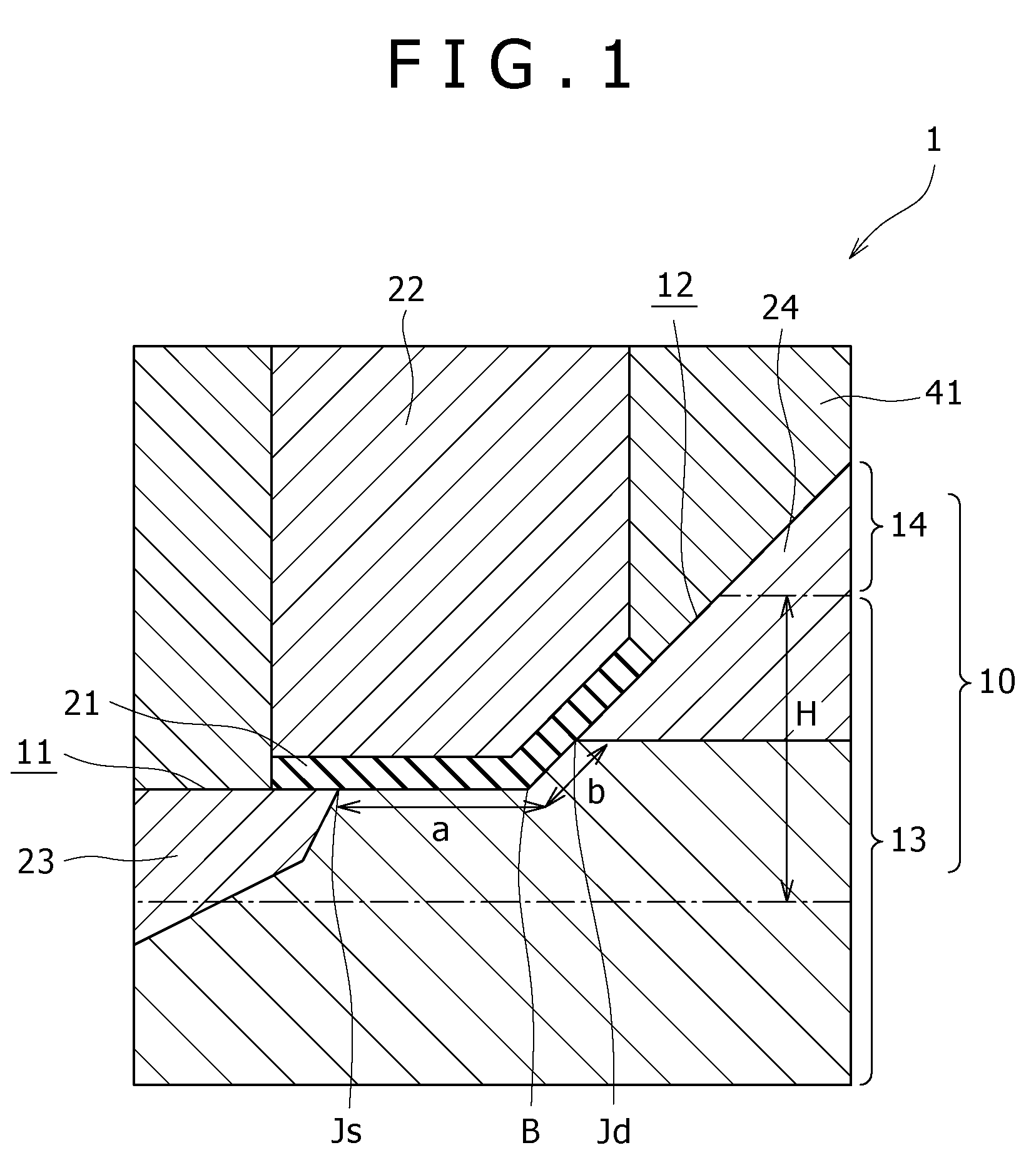
[0060]An embodiment (first embodiment) of a semiconductor device according to an embodiment of the present invention will be described with reference to a schematic constitution sectional view of FIG. 1.

[0061]As shown in FIG. 1, a semiconductor region 10 has a first semiconductor face 11 and a second semiconductor face 12 connected to the first semiconductor face 11 and having an inclination with respect to the first semiconductor face 11. For example, the semiconductor region 10 includes a semiconductor substrate 13 having the first semiconductor face 11 and a semiconductor layer 14 having the second semiconductor face 12 on the semiconductor substrate 13. The second semiconductor face 12 is joined to the first semiconductor face and is formed also on a part of the semiconductor substrate 13. The semiconductor layer 14 is formed by epitaxial growth on the semiconductor substrate 13, for example. It suffices for an interface between the semiconductor layer 14 and the semiconductor s...

second embodiment

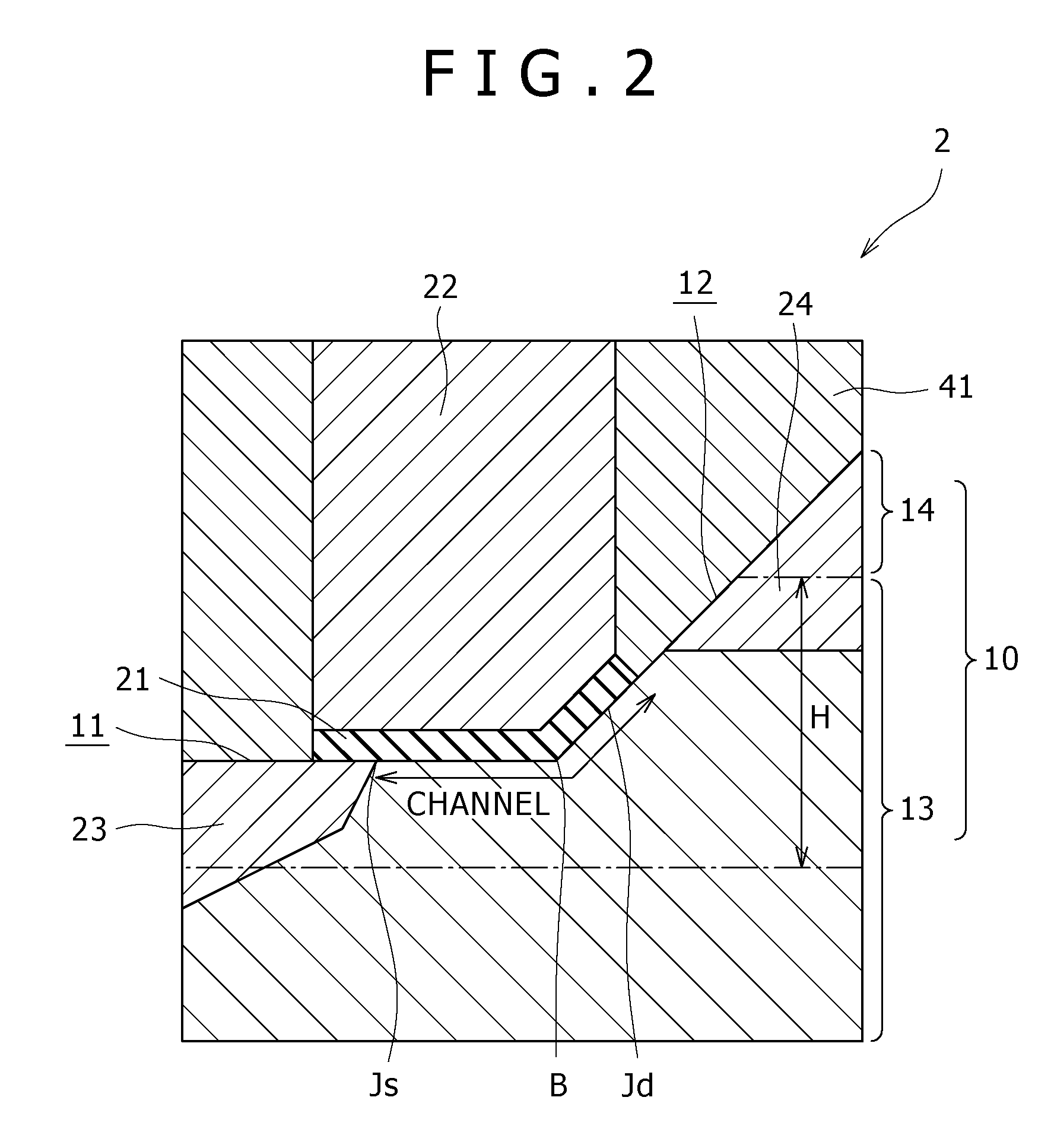
[0068]An embodiment (second embodiment) of the present invention will next be described with reference to a schematic constitution sectional view of FIG. 2.

[0069]As shown in FIG. 2, a semiconductor region 10 has a first semiconductor face 11 and a second semiconductor face 12 connected to the first semiconductor face 11 and having an inclination with respect to the first semiconductor face 11. For example, the semiconductor region 10 includes a semiconductor substrate 13 having the first semiconductor face 11 and a semiconductor layer 14 having the second semiconductor face 12 on the semiconductor substrate 13. The second semiconductor face 12 is joined to the first semiconductor face and is formed also on a part of the semiconductor substrate 13. The semiconductor layer 14 is formed by epitaxial growth on the semiconductor substrate 13, for example. It suffices for an interface between the semiconductor layer 14 and the semiconductor substrate 13 to be within a range H indicated by...

third embodiment

[0076]An embodiment (third embodiment) of the present invention will next be described with reference to a schematic constitution sectional view of FIG. 3.

[0077]As shown in FIG. 3, a semiconductor region 10 has a first semiconductor face 11 and a second semiconductor face 12 connected to the first semiconductor face 11 and having an inclination with respect to the first semiconductor face 11. For example, the semiconductor region 10 includes a semiconductor substrate 13 having the first semiconductor face 11 and a semiconductor layer 14 having the second semiconductor face 12 on the semiconductor substrate 13. The second semiconductor face 12 is joined to the first semiconductor face and is formed also on a part of the semiconductor substrate 13. The semiconductor layer 14 is formed by epitaxial growth on the semiconductor substrate 13, for example. It suffices for an interface between the semiconductor layer 14 and the semiconductor substrate 13 to be within a range H indicated by ...


PUM


Abstract

A semiconductor device including: a semiconductor region having a first semiconductor face and a second semiconductor face connected to the first semiconductor face and having an inclination with respect to the first semiconductor face; a gate insulating film formed on the first and on the second semiconductor faces; a gate electrode formed on the gate insulating film including a part on a boundary between the first semiconductor face and the second semiconductor face; a source impurity region formed in the semiconductor region so as to overlap the gate electrode within the first semiconductor face with the gate insulating film interposed between the source impurity region and the gate electrode; and a drain impurity region formed in the semiconductor region directly under the second semiconductor face at least.

Description

CROSS REFERENCES TO RELATED APPLICATIONS[0001]The present invention contains subject matter related to Japanese Patent Application JP 2006-238626 filed in the Japan Patent Office on Sep. 4, 2006, the entire contents of which being incorporated herein by reference.BACKGROUND OF THE INVENTION[0002]1. Field of the Invention[0003]The present invention relates to an insulated gate field effect transistor, a semiconductor device formed by a static random-access memory using this transistor, and a method of manufacturing the semiconductor device.[0004]2. Description of the Related Art Higher speed, higher levels of integration, and lower power consumption of integrated circuits have heretofore been pursued mainly by scaling down a planar type MOSFET (Metal Oxide Semiconductor Field Effect Transistor). The sectional structure of an existing planar type MOSFET will be described with reference to a schematic constitution sectional view of FIG. 25.[0005]As shown in FIG. 25, the planar type MOS...

Claims


Application Information

Patent Timeline
Patent Type & Authority Applications(United States)
IPC IPC(8): H01L29/94H01L21/336
CPCH01L21/26586H01L29/1037H01L29/6653H01L29/7835H01L29/6659H01L29/66628H01L29/66659H01L29/66545H01L21/18H10B10/00
Inventor IMOTO, TSUTOMUKOBAYASHI, TOSHIOKATO, TAKAYOSHI
Owner SONY CORP
Why Eureka
Try Eureka