Semiconductor on glass insulator made using improved hydrogen reduction process

a technology of glass insulator and semiconductor, which is applied in the manufacture of semiconductor/solid-state devices, basic electric elements, electric devices, etc., can solve the problems of reducing the hydrogen concentration of the substrate, requiring special equipment, and not achieving satisfactory structures in terms of cost and/or bond strength and durability. , to achieve the effect of reducing the concentration of hydrogen

Inactive Publication Date: 2008-03-06
CORNING INC
View PDF11 Cites 36 Cited by
  • Summary
  • Abstract
  • Description
  • Claims
  • Application Information

AI Technical Summary

Benefits of technology

[0009]In accordance with one or more embodiments of the present invention, methods and apparatus of forming a semiconductor on glass structure, include: subjecting an implantation surface of a donor semiconductor wafer to an ion implantation process to create an exfoliation layer of the donor semiconductor wafer; and reducing a concentration of hydrogen at least at the implantation surface of the donor semiconductor wafer using ozonated water.

Problems solved by technology

The former two methods have not resulted in satisfactory structures in terms of cost and / or bond strength and durability.
(Due to the high temperature steps, this process does not work with lower cost glass or glass-ceramic substrates.)
Disadvantageously, the process of subjecting the implantation surface to oxidation, such as oxygen plasma, requires specialized equipment and a complex control of the atmosphere under which oxidation takes place.
This results in relatively high costs, both in terms of time and money.
The cost problem may be significantly exacerbated if high throughput applications are needed or large SOI structure sizes are desired.

Method used


Image

  • Semiconductor on glass insulator made using improved hydrogen reduction process
  • Semiconductor on glass insulator made using improved hydrogen reduction process
  • Semiconductor on glass insulator made using improved hydrogen reduction process

Examples


example 1

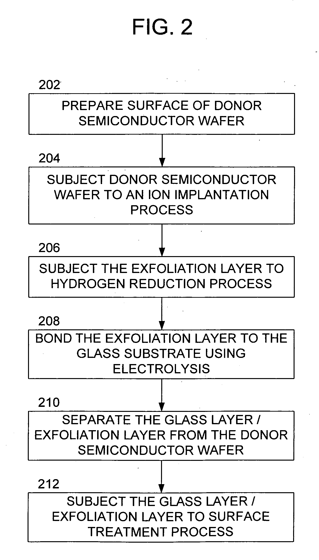
[0053]An experiment was conducted to demonstrate the applicability of the aforementioned hydrogen reducing process on an SiOG structure. A donor semiconductor wafer, a silicon wafer, of 150 mm diameter and 500 microns thick was hydrogen ion implanted at dosage of 8×10¹⁶ ions / cm2 and an implantation energy of 100 KeV. The donor semiconductor wafer was then washed in an automated washer (Akrion) in accordance with the following process: (i) washing the donor semiconductor wafer with a so-called SCl solution (which includes NH4OH,H2O2,H2O at concentrations of 1 part, 2 parts, and 20 parts, respectively) at a temperature of 60° C. for 10 minutes and at 1000 W megasonic agitation; (ii) applying a mixture to the donor semiconductor wafer, where the mixture was hydrofluoric and hydrochloric acid at concentrations of 1 part, 1 part, and 200 parts, respectively) at a temperature of 23° C. for 5 min); and (iii) rinsing the donor semiconductor wafer with ozonated water (at a concentration of 1...

example 2

[0054]The experiment described in EXAMPLE 1 was repeated on a spin / spray tool with equivalent results.

example 3

[0055]A post-polish cleaning experiment was conducted using a spin / spray tool. After slurry removal, the polished substrate was subjected to treatment with ozonated water, the first solution, the second solution, and again with ozonated water. Significant reduction in ionic contamination was measured by ToF SIMS.


PUM


Abstract

Methods and apparatus for producing a semiconductor on glass (SiOG) structure include: subjecting an implantation surface of a donor semiconductor wafer to an ion implantation process to create an exfoliation layer of the donor semiconductor wafer; reducing a concentration of hydrogen at least at the implantation surface of the donor semiconductor wafer using ozonated water; bonding the implantation surface of the exfoliation layer to a glass substrate using electrolysis; and separating the exfoliation layer from the donor semiconductor wafer, thereby exposing at least one cleaved surface.

Description

BACKGROUND[0001]The present invention relates to the manufacture of a semiconductor-on-Insulator (SOI) structure using an improved pre-exfoliation and post-thinning cleaning film process.[0002]To date, the semiconductor material most commonly used in semiconductor-on-insulator structures has been silicon. Such structures have been referred to in the literature as silicon-on-insulator structures and the abbreviation “SOI” has been applied to such structures. SOI technology is becoming increasingly important for high performance thin film transistors, solar cells, and displays, such as, active matrix displays. SOI structures may include a thin layer of substantially single crystal silicon (generally 0.1-0.3 microns in thickness but, in some cases, as thick as 5 microns) on an insulating material.[0003]For ease of presentation, the following discussion will at times be in terms of SOI structures. The references to this particular type of SOI structure are made to facilitate the explana...

Claims


Application Information

Patent Timeline
Patent Type & Authority Applications(United States)
IPC IPC(8): H01L21/00
CPCH01L21/187H01L21/76254
Inventor GADKAREE, KISHOR PURUSHOTTAMMATTHEWS, SUZANNE MARIE
Owner CORNING INC
Why Eureka
Try Eureka